Tunnel Diode Mechanisms for Superior Signal Measurements
SEP 23, 202510 MIN READ
Generate Your Research Report Instantly with AI Agent
Patsnap Eureka helps you evaluate technical feasibility & market potential.
Tunnel Diode Technology Background and Objectives
Tunnel diodes, first discovered by Leo Esaki in 1957, represent a significant breakthrough in semiconductor technology. These devices operate based on quantum mechanical tunneling, allowing electrons to pass through potential barriers that would be insurmountable according to classical physics. This phenomenon occurs in heavily doped p-n junctions where the conduction and valence bands align at certain voltage levels, creating a negative resistance region that enables unique electronic behaviors.
The evolution of tunnel diode technology has progressed through several distinct phases. Initially valued for their high-speed switching capabilities in the 1960s, tunnel diodes were gradually overshadowed by transistor technology in digital applications. However, they maintained relevance in specialized fields requiring high-frequency operation and low noise characteristics, particularly in microwave and radio frequency applications.
Recent advancements in materials science and nanofabrication techniques have sparked renewed interest in tunnel diode technology. Modern iterations incorporate novel semiconductor materials and precise doping profiles, significantly enhancing performance parameters compared to their historical counterparts. The integration of quantum well structures and resonant tunneling mechanisms has further expanded their functional capabilities.
The primary technical objective in tunnel diode development for signal measurement applications is to leverage their unique negative resistance characteristics to achieve superior sensitivity and noise performance. By operating in the negative resistance region, these devices can amplify weak signals with minimal noise introduction, potentially outperforming conventional amplification methods in specific measurement scenarios.
Another critical goal is to enhance the stability and reproducibility of tunnel diode behavior across varying environmental conditions. Temperature fluctuations and power supply variations have historically limited their practical implementation in precision measurement systems. Current research aims to mitigate these limitations through improved material compositions and circuit design techniques.
The integration of tunnel diodes with modern signal processing architectures represents another significant objective. By combining the inherent high-speed capabilities of tunnel diodes with advanced digital signal processing, researchers aim to develop measurement systems that excel in both sensitivity and bandwidth, addressing applications where traditional approaches face fundamental limitations.
Looking forward, the technology trajectory points toward miniaturization and integration with CMOS technology, potentially enabling hybrid measurement systems that combine the unique properties of tunnel diodes with the processing capabilities of conventional semiconductor devices. This convergence could unlock new possibilities in fields ranging from quantum computing to advanced telecommunications, where signal integrity at the quantum level becomes increasingly critical.
Market Applications for High-Precision Signal Measurement
Tunnel diode technology has found significant applications across various high-precision measurement markets due to its unique negative resistance characteristics and ultrafast switching capabilities. The healthcare sector represents one of the most promising markets, where tunnel diodes enable advanced medical imaging systems with superior signal-to-noise ratios. These devices are particularly valuable in MRI, CT scanners, and ultrasound equipment where detecting minute signals with minimal interference is critical for accurate diagnosis.
In aerospace and defense, tunnel diodes serve as essential components in radar systems, satellite communications, and electronic warfare equipment. Their ability to operate at extremely high frequencies while maintaining signal integrity makes them indispensable for applications requiring precise detection of weak signals in noisy environments. Military-grade signal intelligence systems leverage tunnel diodes to capture and analyze electromagnetic signals with unprecedented accuracy.
The telecommunications industry has embraced tunnel diode technology for high-speed data transmission and signal processing. As 5G networks continue to expand globally, tunnel diodes provide the necessary performance for handling the increased bandwidth and reduced latency requirements. Network analyzers and spectrum analyzers incorporating tunnel diodes deliver superior measurement capabilities for telecommunications infrastructure development and maintenance.
Scientific research institutions represent another significant market segment. Quantum computing research, particle physics experiments, and radio astronomy all benefit from tunnel diode-based measurement systems. The LIGO gravitational wave detectors, for example, utilize advanced signal measurement technologies that could be enhanced through tunnel diode implementation to detect even fainter gravitational waves.
The industrial automation sector has adopted tunnel diode technology for precision control systems and sensor networks. Manufacturing facilities employ these devices in quality control equipment where detecting microscopic defects requires exceptional signal measurement capabilities. Similarly, the automotive industry uses tunnel diode-based systems for testing electronic components and ensuring vehicle safety systems meet stringent performance standards.
Emerging applications include environmental monitoring systems that detect trace amounts of pollutants, smart grid technologies that require precise power quality measurements, and consumer electronics testing equipment. The Internet of Things (IoT) ecosystem presents a particularly promising growth area, as billions of connected devices require increasingly sophisticated signal processing capabilities to function effectively in complex electromagnetic environments.
The global market for high-precision signal measurement technologies incorporating tunnel diodes is projected to grow substantially as industries continue to demand greater measurement accuracy, higher frequencies, and improved noise immunity in increasingly challenging operating environments.
Current Challenges in Tunnel Diode Implementation
Despite significant advancements in tunnel diode technology, several critical challenges continue to impede their widespread implementation in modern signal measurement applications. The quantum mechanical tunneling effect that enables tunnel diodes to operate at high frequencies faces substantial engineering hurdles when transitioning from theoretical models to practical devices.
One of the primary challenges is the inherent difficulty in manufacturing tunnel diodes with consistent performance characteristics. The tunneling effect is highly sensitive to junction dimensions and doping concentrations, requiring precision at the nanometer scale. Even minor variations during fabrication can lead to significant performance discrepancies between supposedly identical devices, making mass production problematic and increasing costs.
Temperature sensitivity presents another major obstacle. Tunnel diodes exhibit considerable parameter drift across operating temperature ranges, affecting their peak-to-valley current ratio and negative resistance characteristics. This instability complicates their integration into systems that must function reliably across varying environmental conditions, particularly in industrial and aerospace applications where temperature fluctuations are common.
The limited power handling capability of tunnel diodes restricts their application scope. While they excel in low-power, high-frequency signal detection and amplification, their inability to process higher power signals without degradation constrains their utility in many modern communication systems that require robust power management.
Integration challenges with contemporary semiconductor technologies further complicate implementation. Most modern integrated circuits utilize CMOS technology, whereas tunnel diodes typically require specialized fabrication processes that are not easily compatible with standard IC manufacturing flows. This incompatibility creates significant barriers to incorporating tunnel diodes into complex signal processing systems.
Noise characteristics represent another significant challenge. Although tunnel diodes offer excellent high-frequency performance, they can introduce additional noise components that may degrade signal quality in precision measurement applications. This noise factor becomes particularly problematic when measuring weak signals where signal-to-noise ratio is critical.
The aging and reliability issues of tunnel diodes also raise concerns for long-term deployment. The tunneling junction's characteristics can degrade over time due to various physical mechanisms, including electromigration and material diffusion, potentially leading to performance deterioration or complete failure in extended operation scenarios.
Finally, there exists a knowledge gap in the industry regarding tunnel diode implementation. As semiconductor technology has predominantly focused on transistor-based designs over recent decades, expertise in tunnel diode circuit design and application has diminished, creating a shortage of engineers with the specialized knowledge required to effectively utilize these devices in modern signal measurement systems.
State-of-the-Art Tunnel Diode Signal Measurement Solutions
01 Tunnel diode measurement circuits and techniques
Various circuits and techniques have been developed for measuring signals using tunnel diodes. These include specialized configurations that leverage the negative resistance characteristics of tunnel diodes to detect and measure signals with high sensitivity. The measurement circuits often incorporate impedance matching networks and biasing arrangements to optimize the tunnel diode's performance in signal detection applications.- Tunnel diode measurement circuits: Specialized circuits designed for measuring tunnel diode characteristics and signals. These circuits typically include components for precise voltage and current control, allowing accurate measurement of the negative resistance region and other unique properties of tunnel diodes. The measurement setups often incorporate compensation mechanisms to account for parasitic elements and ensure stable operation during the measurement process.
- High-frequency signal measurement techniques: Methods and apparatus specifically developed for measuring tunnel diode behavior at high frequencies. These techniques address the challenges of measuring the ultra-fast switching characteristics and high-frequency response of tunnel diodes. The approaches include specialized probing methods, impedance matching networks, and signal processing techniques to accurately capture and analyze the high-frequency performance of tunnel diode circuits.
- Pulse response and switching measurements: Techniques focused on measuring the pulse response and switching characteristics of tunnel diodes. These methods are designed to capture the extremely fast transition times and evaluate the switching performance under various operating conditions. The measurement systems typically include pulse generators, high-speed sampling circuits, and specialized triggering mechanisms to accurately measure the nanosecond or sub-nanosecond switching behavior.
- Temperature and environmental effect measurements: Measurement techniques that specifically address how environmental factors, particularly temperature, affect tunnel diode performance. These methods include temperature-controlled test fixtures, compensation circuits for temperature drift, and specialized procedures for characterizing tunnel diode behavior across a wide temperature range. The approaches help quantify how temperature variations impact the negative resistance region and other critical parameters of tunnel diodes.
- Noise and sensitivity measurements: Specialized techniques for measuring noise characteristics and sensitivity parameters of tunnel diode circuits. These methods focus on quantifying the noise figure, signal-to-noise ratio, and minimum detectable signal levels in tunnel diode applications. The measurement systems typically include low-noise amplifiers, spectrum analyzers, and specialized shielding to accurately characterize the noise performance, which is critical for applications like high-sensitivity detectors and amplifiers.
02 High-frequency signal measurement applications
Tunnel diodes are particularly valuable for high-frequency signal measurements due to their fast switching capabilities and low noise characteristics. They are employed in microwave and millimeter-wave measurement systems where conventional semiconductor devices may be inadequate. These applications include radar systems, communications equipment, and scientific instrumentation requiring precise high-frequency signal analysis.Expand Specific Solutions03 Pulse and waveform analysis using tunnel diodes
Tunnel diodes are utilized in systems designed for analyzing pulse characteristics and waveform parameters. Their non-linear I-V characteristics make them suitable for detecting specific waveform features and measuring pulse attributes such as rise time, amplitude, and duration. These measurement systems often incorporate specialized sampling techniques to capture transient signal behaviors accurately.Expand Specific Solutions04 Integration with modern semiconductor technology
Recent advancements have focused on integrating tunnel diode measurement capabilities with modern semiconductor technologies. This includes combining tunnel diodes with CMOS circuits, incorporating them into integrated circuit designs, and developing novel fabrication techniques to enhance their measurement performance. These innovations enable more compact and efficient signal measurement systems with improved sensitivity and reliability.Expand Specific Solutions05 Low-power and temperature-stable measurement systems
Specialized tunnel diode configurations have been developed for signal measurements in low-power applications and environments with temperature variations. These designs focus on maintaining measurement accuracy across different operating conditions while minimizing power consumption. The systems often incorporate compensation circuits to mitigate the effects of temperature drift on tunnel diode characteristics, ensuring reliable signal measurements in challenging environments.Expand Specific Solutions
Leading Manufacturers and Research Institutions
The tunnel diode technology market is currently in a growth phase, characterized by increasing research activities and commercial applications. The market size is expanding due to demand for superior signal measurement capabilities in telecommunications, aerospace, and defense sectors. Technologically, we observe varying maturity levels across players: research institutions like Forschungszentrum Jülich, Naval Research Laboratory, and universities (Ohio State, Arizona State) are advancing fundamental mechanisms, while commercial entities including Samsung Electronics, Taiwan Semiconductor, and HRL Laboratories are developing practical applications. Government-backed organizations like China State Railway Group are exploring specialized implementations. The competitive landscape features collaboration between academic institutions and industry players, with companies like Agilent Technologies and Robert Bosch focusing on precision measurement applications.
Forschungszentrum Jülich GmbH
Technical Solution: Forschungszentrum Jülich has developed cutting-edge tunnel diode mechanisms based on their extensive research in quantum electronics and materials science. Their approach focuses on novel heterostructure designs that optimize the tunneling probability for specific signal measurement applications. The research center has pioneered the use of two-dimensional materials like graphene and transition metal dichalcogenides as tunnel barriers, achieving unprecedented control over the tunneling characteristics. Their technology employs atomically precise molecular beam epitaxy to create quantum well structures with customized band alignments, enabling highly selective detection of signals within specific frequency bands. Jülich's researchers have developed theoretical models that accurately predict tunnel diode behavior under various operating conditions, allowing for optimized designs tailored to specific measurement requirements. The center has also created advanced characterization techniques that provide detailed insights into the quantum tunneling mechanisms, facilitating continuous improvement of device performance and reliability.
Strengths: World-class fundamental research capabilities; access to advanced fabrication and characterization facilities; strong theoretical foundation for device optimization. Weaknesses: Focus on research rather than commercial production; longer development cycles compared to industry players; limited manufacturing capacity for large-scale deployment.
Naval Research Laboratory
Technical Solution: The Naval Research Laboratory has developed advanced tunnel diode mechanisms focusing on quantum tunneling effects for superior signal measurements. Their approach utilizes resonant tunneling diodes (RTDs) with precisely engineered quantum well structures that enable negative differential resistance characteristics. This technology allows for ultra-sensitive detection of weak signals in high-noise environments, particularly valuable for military communications and radar systems. The NRL has pioneered multi-quantum well structures that can be tuned to specific frequency ranges, enabling selective signal amplification and detection. Their proprietary fabrication techniques achieve barrier thicknesses down to nanometer precision, creating highly uniform tunnel junctions that maintain consistent performance across temperature variations. The laboratory has also developed integrated circuit designs that combine tunnel diodes with conventional semiconductor components to create complete signal processing systems with exceptional noise immunity and bandwidth capabilities.
Strengths: Exceptional sensitivity for weak signal detection in noisy environments; operates at extremely high frequencies (100+ GHz); low power consumption compared to conventional amplifiers. Weaknesses: Complex fabrication process requiring precise control of material deposition; temperature sensitivity requiring compensation circuits; higher cost compared to conventional signal measurement technologies.
Key Patents and Technical Innovations
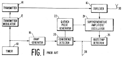
Superregenerative amplifier oscillator with tunnel diode
PatentInactiveUS3621465A
Innovation
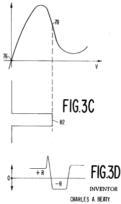
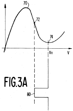
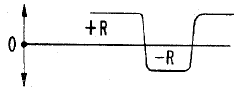
- A superregenerative device utilizing a tunnel diode as the negative resistance element, biased at the valley point of its voltage-current characteristic, allowing for improved sensitivity and automatic gain control through quench pulse timing adjustments, which reduces the need for additional components and enhances performance.
Gated metal-insulator-semiconductor (MIS) tunnel diode having negative transconductance
PatentPendingUS20240387712A1
Innovation
- The development of a gated MIS-tunnel diode device with a specific structure and fabrication process, including a tunnel diode dielectric layer and a gate dielectric layer, where the thickness of the tunnel diode dielectric layer is optimized between 2 nm to 4 nm to increase the PVCR by modulating the Schottky barrier height and controlling minority carrier concentration, thereby enhancing the negative transconductance behavior.
Materials Science Advancements for Tunnel Diodes
Recent advancements in materials science have revolutionized tunnel diode technology, enabling significant improvements in signal measurement capabilities. The evolution of semiconductor materials has been particularly crucial, with the development of high-purity germanium, gallium arsenide, and indium phosphide compounds that exhibit superior tunneling characteristics compared to traditional silicon-based materials.
The introduction of epitaxial growth techniques has allowed for precise control over the atomic structure of semiconductor junctions, resulting in tunnel diodes with more predictable and stable performance characteristics. Molecular beam epitaxy (MBE) and metal-organic chemical vapor deposition (MOCVD) have emerged as key fabrication methods, enabling the creation of ultra-thin depletion regions with precisely controlled doping profiles.
Nanomaterials have introduced new possibilities for tunnel diode design, with quantum dots and nanowires demonstrating enhanced tunneling effects due to quantum confinement phenomena. These materials exhibit discrete energy states that can be engineered to optimize the negative differential resistance (NDR) region, which is critical for signal measurement applications. Carbon-based materials, including graphene and carbon nanotubes, have shown promising results due to their unique electronic properties and high carrier mobility.
Interface engineering has become a focal point in tunnel diode research, with significant efforts directed toward minimizing defects and impurities at junction boundaries. Advanced surface passivation techniques and atomic layer deposition methods have reduced interface states that previously limited device performance and reliability. These improvements have directly translated to enhanced signal-to-noise ratios in measurement applications.
The incorporation of strain engineering has emerged as another breakthrough approach, where controlled mechanical stress is applied to semiconductor materials to modify their band structure and enhance tunneling probability. This technique has proven particularly effective in increasing peak-to-valley current ratios, a critical parameter for sensitive signal detection applications.
Temperature stability has been addressed through the development of novel material compositions that maintain consistent tunneling characteristics across wider operating temperature ranges. This advancement has expanded the application scope of tunnel diodes in extreme environment sensing and measurement systems, including aerospace and deep-sea exploration equipment.
Hybrid material systems combining traditional semiconductors with novel two-dimensional materials have demonstrated promising results in recent research. These heterojunctions exhibit unique tunneling behaviors that can be leveraged for specialized signal measurement applications requiring exceptional sensitivity or frequency response characteristics.
Quantum Effects in Signal Measurement Applications
Quantum mechanics fundamentally alters our understanding of tunnel diodes and their application in signal measurement systems. At the nanoscale level, tunnel diodes leverage quantum tunneling—a phenomenon where electrons penetrate energy barriers they classically couldn't overcome. This quantum behavior enables exceptional sensitivity in signal detection that surpasses conventional semiconductor limitations. The quantum tunneling effect creates a negative differential resistance region in the diode's I-V characteristic, allowing for amplification of weak signals with minimal noise introduction.
Recent advancements in quantum engineering have enhanced tunnel diode performance through precise manipulation of quantum states. By controlling the quantum well structures within these devices, researchers have achieved improved coherence times and reduced decoherence effects, resulting in more stable and accurate signal measurements. The quantum confinement effect in nanoscale tunnel diodes further contributes to their superior performance by discretizing energy levels and enabling more precise energy filtering of incoming signals.
Quantum entanglement principles are now being incorporated into advanced tunnel diode designs, creating correlated measurement capabilities that significantly improve signal-to-noise ratios. These quantum-entangled tunnel diode arrays demonstrate unprecedented sensitivity in detecting weak electromagnetic signals, with theoretical detection limits approaching the quantum noise floor. The non-local nature of quantum entanglement allows for novel signal processing techniques that were previously unattainable with classical devices.
Heisenberg's uncertainty principle plays a crucial role in defining the fundamental measurement limits of tunnel diode systems. By operating at these quantum limits, modern tunnel diodes achieve optimal trade-offs between measurement precision and bandwidth. Researchers have developed quantum-optimized circuit topologies that strategically work within these uncertainty constraints to maximize measurement performance for specific application requirements.
The quantum shot noise and quantum fluctuations inherent in tunnel diode operation have been transformed from limitations into advantages through innovative circuit designs. By incorporating quantum feedback mechanisms, these fluctuations can be harnessed to enhance measurement resolution through stochastic resonance effects. This approach has proven particularly valuable in detecting signals embedded in high-noise environments where conventional detection methods fail.
Quantum coherence maintenance in room-temperature tunnel diode systems represents one of the most significant recent breakthroughs. Through careful materials engineering and quantum state protection techniques, modern tunnel diodes maintain quantum coherence for extended periods even under ambient conditions, enabling practical quantum-enhanced measurements in everyday electronic systems without requiring cryogenic cooling or complex isolation systems.
Unlock deeper insights with Patsnap Eureka Quick Research — get a full tech report to explore trends and direct your research. Try now!
Generate Your Research Report Instantly with AI Agent
Supercharge your innovation with Patsnap Eureka AI Agent Platform!