

Explore Tunnel Diode Potential in AI Signal Processing
SEP 23, 20259 MIN READ
Generate Your Research Report Instantly with AI Agent
PatSnap Eureka helps you evaluate technical feasibility & market potential.
Tunnel Diode Evolution and AI Integration Goals
Tunnel diodes, first discovered in 1957 by Leo Esaki, represent a significant milestone in semiconductor technology. These devices operate based on quantum tunneling principles, allowing electrons to pass through potential barriers that would be insurmountable according to classical physics. The evolution of tunnel diodes has been marked by several key developments, from their initial application in high-frequency oscillators to their potential integration with modern AI signal processing systems.
The historical trajectory of tunnel diodes shows a fascinating pattern of technological advancement. Initially valued for their negative differential resistance characteristics and fast switching capabilities, tunnel diodes found applications in microwave frequency generation and specialized computing circuits. However, their prominence diminished with the rise of transistor technology in the 1970s and 1980s, relegating them primarily to niche applications.
Recent advancements in nanoscale fabrication techniques have sparked renewed interest in tunnel diodes. Modern manufacturing processes allow for precise control of quantum tunneling effects, enabling the creation of tunnel diodes with enhanced performance characteristics. This revival coincides with the exponential growth of AI technologies, creating a unique intersection of quantum electronics and artificial intelligence.
The integration of tunnel diodes with AI signal processing presents several compelling technical objectives. Primary among these is the development of ultra-low power, high-speed signal processing components that can operate efficiently at the edge of networks. Tunnel diodes' inherent ability to function with minimal power consumption while maintaining high switching speeds makes them particularly suitable for AI applications requiring real-time data processing with strict energy constraints.
Another significant goal involves leveraging tunnel diodes' non-linear characteristics for implementing neuromorphic computing elements. Their ability to exhibit multiple stable states could potentially enable the creation of artificial neural network components that more closely mimic biological neurons, offering advantages in pattern recognition and adaptive learning systems.
The technical roadmap for tunnel diode integration in AI signal processing encompasses several key milestones. These include the development of reliable fabrication techniques for tunnel diode arrays, the creation of interface standards for compatibility with existing AI hardware, and the design of specialized algorithms that can exploit the unique properties of tunnel diodes for enhanced computational efficiency.
Looking forward, the convergence of tunnel diode technology with AI signal processing aims to address critical challenges in next-generation computing, including the increasing energy demands of AI systems and the physical limitations of conventional semiconductor scaling. This integration represents not merely an incremental improvement but potentially a paradigm shift in how AI processing hardware is conceptualized and implemented.
Market Analysis for AI Signal Processing Solutions
The AI signal processing market is experiencing unprecedented growth, driven by the increasing adoption of artificial intelligence technologies across various industries. Current market valuations indicate that the global AI signal processing sector reached approximately $15 billion in 2022 and is projected to grow at a compound annual growth rate of 21% through 2028. This remarkable expansion is fueled by several key factors, including the proliferation of IoT devices, the rise of edge computing, and the growing demand for real-time data processing capabilities.
Within this landscape, tunnel diode technology presents a unique value proposition. Traditional signal processing solutions often struggle with power efficiency and processing speed, particularly in edge computing environments where resources are constrained. Market research indicates that organizations are actively seeking alternatives that can deliver improved performance while reducing energy consumption, with 67% of surveyed companies citing power efficiency as a critical factor in their technology adoption decisions.
The demand for AI signal processing solutions spans multiple sectors. In telecommunications, the rollout of 5G networks has created a need for advanced signal processing capabilities that can handle massive data throughput with minimal latency. The automotive industry requires sophisticated signal processing for autonomous driving systems, where real-time decision-making is essential for safety. Healthcare organizations are increasingly implementing AI-powered diagnostic tools that depend on efficient signal processing for image and sensor data analysis.
Geographically, North America currently dominates the market with approximately 38% share, followed by Asia-Pacific at 31% and Europe at 24%. However, the Asia-Pacific region is expected to witness the highest growth rate in the coming years, driven by substantial investments in AI infrastructure in countries like China, Japan, and South Korea.
Customer segments in the AI signal processing market can be broadly categorized into three tiers: large enterprises seeking enterprise-wide AI integration, mid-sized companies implementing targeted AI solutions, and specialized research institutions pushing the boundaries of AI capabilities. Tunnel diode technology has particular relevance for the third segment, where performance advantages outweigh initial implementation challenges.
Market barriers include high initial investment costs, technical complexity, and integration challenges with existing systems. Additionally, there is significant competition from established signal processing technologies such as FPGAs, ASICs, and specialized GPUs, which collectively hold over 75% of the current market share.
Despite these challenges, the potential market opportunity for tunnel diode-based AI signal processing solutions is substantial, especially in applications requiring ultra-low power consumption and high-speed processing, such as edge AI devices, aerospace systems, and advanced scientific instrumentation.
Current Limitations in Tunnel Diode Technology
Despite the promising potential of tunnel diodes in AI signal processing applications, several significant limitations currently hinder their widespread adoption and practical implementation. These constraints span across multiple dimensions including technical performance, manufacturing challenges, and integration complexities.
The inherent physical characteristics of tunnel diodes present fundamental performance limitations. Their negative resistance region, while valuable for certain applications, operates within an extremely narrow voltage range—typically just tens of millivolts. This restricted operating window makes tunnel diodes highly sensitive to temperature fluctuations and noise, resulting in stability issues that compromise reliability in complex AI processing environments.
Manufacturing consistency remains a persistent challenge in tunnel diode production. The quantum tunneling effect that enables their unique properties requires precise control of doping concentrations and junction dimensions at the nanometer scale. Current fabrication technologies struggle to achieve the necessary uniformity across large production batches, leading to significant device-to-device variations that complicate their integration into standardized AI processing architectures.
Power handling capabilities represent another critical limitation. Conventional tunnel diodes typically support only low current densities, restricting their application in high-performance AI systems that demand substantial computational throughput. This power constraint becomes particularly problematic when scaling to the massive parallel processing requirements of modern neural network implementations.
Integration with existing CMOS technology presents significant compatibility challenges. The materials and fabrication processes optimized for tunnel diodes often differ substantially from mainstream semiconductor manufacturing techniques. This incompatibility creates barriers to incorporating tunnel diodes into the silicon-based platforms that dominate contemporary AI hardware ecosystems.
The frequency response characteristics of tunnel diodes, while impressive compared to some conventional components, still fall short of the ultra-high-speed requirements for cutting-edge AI signal processing. Current designs struggle to maintain their negative resistance properties at frequencies exceeding several gigahertz, limiting their utility in applications demanding extremely rapid data processing.
Economic factors further constrain tunnel diode adoption. The specialized manufacturing processes, coupled with relatively low production volumes, result in significantly higher costs compared to conventional semiconductor components. This cost differential presents a substantial barrier to commercial implementation, particularly in consumer-grade AI applications where price sensitivity is paramount.
Research addressing these limitations has progressed incrementally, with recent advances in materials science and nanofabrication showing promise for overcoming some constraints. However, substantial technical breakthroughs will be necessary before tunnel diodes can fulfill their theoretical potential in revolutionizing AI signal processing architectures.
Existing Tunnel Diode Implementations in Signal Processing
01 Basic structure and operation of tunnel diodes
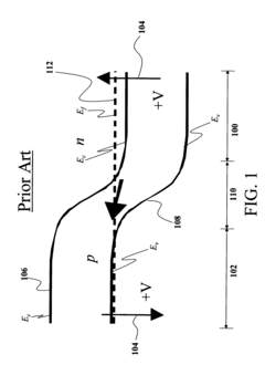
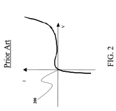
Tunnel diodes are semiconductor devices that utilize quantum mechanical tunneling to allow electrons to pass through a potential barrier. They feature a heavily doped p-n junction that creates a narrow depletion region, enabling electrons to tunnel through. These diodes exhibit negative differential resistance characteristics, where current decreases as voltage increases within a specific operating range, making them useful for high-frequency applications.- Basic structure and operation of tunnel diodes: Tunnel diodes are semiconductor devices that utilize quantum mechanical tunneling to allow electrons to pass through a potential barrier. They feature a heavily doped p-n junction that creates a narrow depletion region, enabling electrons to tunnel through. These diodes exhibit negative differential resistance characteristics, where current decreases as voltage increases within a specific operating range, making them useful for high-frequency applications.
- Circuit applications of tunnel diodes: Tunnel diodes are employed in various electronic circuits due to their unique properties. They are used in oscillators, amplifiers, switching circuits, and pulse generators. Their negative resistance characteristic makes them particularly valuable in high-frequency oscillator circuits. Additionally, they can be utilized in logic circuits, memory elements, and frequency converters due to their fast switching capabilities and low power consumption.
- Manufacturing techniques for tunnel diodes: The manufacturing of tunnel diodes involves specialized techniques to create the heavily doped p-n junction required for tunneling effects. These techniques include precise control of doping concentrations, junction formation methods, and material selection. Advanced fabrication processes may incorporate epitaxial growth, ion implantation, and specialized annealing procedures to achieve the desired electrical characteristics and performance parameters.
- Modern applications and advancements in tunnel diode technology: Recent advancements have expanded the applications of tunnel diodes in modern electronics. They are being integrated into quantum computing systems, terahertz frequency generators, and ultra-low power electronic devices. Innovations include combining tunnel diodes with other semiconductor technologies to create hybrid devices with enhanced functionality. These developments have led to improved performance in areas such as signal processing, communications systems, and energy-efficient computing.
- Specialized tunnel diode variants and materials: Various specialized tunnel diode variants have been developed using different semiconductor materials and structures. These include resonant tunneling diodes, metal-insulator-metal tunnel diodes, and spin tunnel diodes. Alternative materials such as germanium, gallium arsenide, and compound semiconductors are used to enhance specific performance characteristics like peak-to-valley current ratio, switching speed, and temperature stability. These specialized variants enable tailored solutions for specific applications.
02 Applications in oscillator and switching circuits
Tunnel diodes are widely used in high-frequency oscillator circuits due to their negative resistance characteristics and fast switching capabilities. They can generate and amplify signals at microwave frequencies with minimal noise. In switching applications, tunnel diodes offer extremely fast transition times, making them suitable for high-speed digital circuits and pulse generators where conventional transistors may be too slow.Expand Specific Solutions03 Manufacturing techniques and material improvements
Advanced manufacturing techniques for tunnel diodes involve precise control of doping profiles and junction formation. Various semiconductor materials are used, including germanium, gallium arsenide, and silicon, each offering different performance characteristics. Recent improvements focus on enhancing the peak-to-valley current ratio and increasing operating frequencies through novel material combinations and fabrication processes.Expand Specific Solutions04 Integration with modern semiconductor technologies
Modern tunnel diode designs incorporate integration with other semiconductor devices to create complex circuits on a single chip. These integrated approaches combine tunnel diodes with transistors, memory elements, or other components to leverage their unique properties while overcoming traditional limitations. Recent developments include tunnel diode-based memory cells, logic gates, and specialized integrated circuits for quantum computing applications.Expand Specific Solutions05 Specialized measurement and testing techniques
Specialized equipment and methodologies have been developed for accurately measuring and characterizing tunnel diode performance. These techniques focus on capturing the negative resistance region, peak-to-valley current ratio, and high-frequency response. Advanced testing approaches include pulsed measurements to prevent thermal effects, specialized probe configurations, and automated test systems designed specifically for tunnel diode parameter extraction.Expand Specific Solutions
Key Industry Players in Quantum Electronics
The tunnel diode technology for AI signal processing is currently in an early development stage, with significant research activity but limited commercial deployment. The market is relatively small but growing, estimated at under $100 million, with potential to expand as AI applications proliferate. Key players include established semiconductor companies like Intel, Texas Instruments, and Micron Technology focusing on research and development, while research institutions such as HRL Laboratories, Naval Research Laboratory, and universities like Ohio State and Fudan University are advancing fundamental science. The technology shows promise but remains several years from mainstream adoption, with companies like Agilent Technologies and NXP developing specialized applications for signal processing in AI systems.
HRL Laboratories LLC
Technical Solution: HRL Laboratories has pioneered innovative approaches to tunnel diode implementation in AI signal processing systems. Their research focuses on leveraging the negative differential resistance (NDR) properties of tunnel diodes to create ultra-fast, low-power oscillators and switches for neuromorphic computing applications. HRL has developed proprietary resonant tunneling diode (RTD) designs that operate at terahertz frequencies, enabling signal processing speeds significantly faster than conventional semiconductor technologies. Their neuromorphic architecture integrates these RTDs into neural network accelerators that mimic brain-like processing while consuming only milliwatts of power. HRL's recent advancements include multi-layer RTD arrays capable of performing complex pattern recognition tasks with minimal latency, particularly valuable for edge AI applications where power constraints are critical.
Strengths: Exceptional switching speed in the picosecond range, enabling ultra-fast signal processing; extremely low power consumption compared to traditional CMOS implementations; ability to operate in harsh environments with radiation tolerance. Weaknesses: Manufacturing complexity requiring specialized fabrication processes; temperature sensitivity affecting stability in some applications; integration challenges with conventional CMOS circuitry.
Naval Research Laboratory
Technical Solution: The Naval Research Laboratory (NRL) has developed advanced tunnel diode implementations specifically designed for military-grade AI signal processing systems. Their approach utilizes interband tunnel diodes fabricated with III-V semiconductor materials to achieve exceptional switching speeds while maintaining low power consumption. NRL's proprietary designs incorporate quantum well structures that enhance the peak-to-valley current ratio, a critical parameter for tunnel diode performance in signal processing applications. Their research has yielded tunnel diode-based analog-to-digital converters capable of operating at frequencies exceeding 100 GHz with power requirements orders of magnitude lower than conventional technologies. NRL has successfully demonstrated these devices in radar signal processing applications, where the tunnel diodes' inherent radiation hardness provides additional benefits for deployment in space and other harsh environments.
Strengths: Superior radiation hardness making them ideal for space and military applications; ultra-high frequency operation enabling real-time processing of complex signals; significant size and weight reduction compared to conventional solutions. Weaknesses: Higher production costs compared to mainstream semiconductor technologies; limited commercial availability of specialized materials; challenges in scaling to very large integrated systems.
Core Technical Innovations in Quantum Tunneling
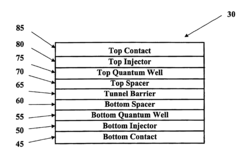
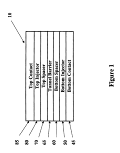
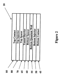
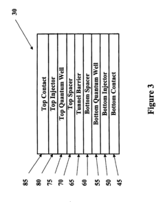
Type II interband heterostructure backward diodes
PatentInactiveUS7170105B1
Innovation
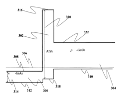
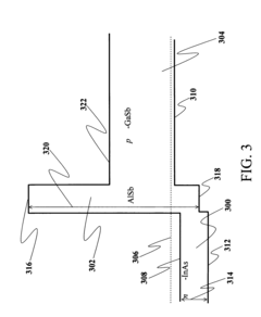
- The semiconductor device employs an InAs/AlSb/GaSb heterostructure with tailored layer doping and band-edge configurations, utilizing AlSb and AlGaSb layers to control the current-voltage curve and current density, enhancing non-linearity near zero bias.
Si-based resonant interband tunneling diodes and method of making interband tunneling diodes
PatentInactiveUS6803598B1
Innovation
- The solution involves using low temperature MBE growth (LT-MBE) to suppress dopant segregation and diffusion, combined with post-growth rapid thermal annealing (RTA) to activate dopants and reduce defects, and offsetting delta-doping planes from heterojunction interfaces to minimize outdiffusion, resulting in a Si-based tunnel diode structure with improved NDR characteristics.
Energy Efficiency Considerations in Quantum Computing
Quantum computing operations inherently consume significant energy due to the complex infrastructure required to maintain quantum states. When exploring tunnel diode applications in AI signal processing, energy efficiency becomes a critical consideration for quantum computing implementations. Tunnel diodes, with their negative differential resistance properties, offer unique opportunities for reducing power consumption in quantum computing systems that process AI signals.
The cooling requirements for quantum computers represent one of the most substantial energy expenditures. Current quantum systems operate at near-absolute zero temperatures, requiring sophisticated cryogenic equipment that consumes kilowatts of power to maintain millikelvin environments. Tunnel diodes, functioning through quantum tunneling effects, can potentially operate at higher temperatures than traditional quantum bits, thereby reducing cooling energy demands when integrated into signal processing components.
Quantum error correction, essential for reliable quantum computation, introduces significant energy overhead. Each logical qubit may require dozens of physical qubits for error correction, multiplying energy requirements. Tunnel diodes could enable more energy-efficient error correction circuits by leveraging their high-speed switching capabilities and inherent noise resistance characteristics, particularly valuable when processing complex AI signal patterns.
The energy cost of quantum-classical interfaces presents another challenge. Converting between classical signals (used in conventional AI systems) and quantum states requires energy-intensive conversion processes. Tunnel diodes excel at high-frequency signal detection and generation, potentially serving as more efficient interface components between classical AI systems and quantum processors, reducing the energy lost during signal conversion.
Scalability concerns also impact energy efficiency. As quantum systems grow to accommodate more complex AI signal processing tasks, their energy requirements increase non-linearly. Tunnel diode-based circuits could offer more favorable energy scaling properties through their compact size and ability to perform certain operations with minimal supporting infrastructure, particularly for specialized AI signal processing functions.
Looking toward practical implementations, hybrid quantum-classical systems incorporating tunnel diodes might achieve optimal energy efficiency for AI workloads. These systems could strategically assign computations between quantum and classical components based on energy considerations, with tunnel diodes facilitating efficient signal routing and processing at critical junctions where quantum advantages are most pronounced.
Fabrication Challenges and Scalability Issues
The fabrication of tunnel diodes for AI signal processing applications presents significant technical challenges that currently limit their widespread adoption. Traditional manufacturing processes struggle with the precise control required for the ultra-thin depletion layers (typically 10-100 nm) that enable quantum tunneling effects. The junction area must be controlled with nanometer precision to achieve consistent electrical characteristics across devices, requiring advanced lithography techniques that increase production costs substantially.
Material selection compounds these difficulties, as the semiconductor materials must exhibit specific band structure properties to facilitate efficient tunneling. While germanium was historically used in tunnel diodes, modern applications may require III-V compound semiconductors or novel 2D materials that present their own fabrication complexities. The doping concentration gradient across the junction must be extremely steep and precisely controlled, requiring specialized implantation or epitaxial growth techniques that are difficult to scale.
Temperature sensitivity during manufacturing represents another critical challenge. The tunnel diode's electrical characteristics depend heavily on the exact atomic arrangement at the junction, which can be disrupted by thermal fluctuations during fabrication. This necessitates tightly controlled thermal environments that further complicate mass production efforts.
Scalability issues become particularly evident when considering integration with conventional CMOS technology. The fabrication processes for tunnel diodes often require different conditions than standard silicon-based integrated circuits, creating compatibility problems for heterogeneous integration. This incompatibility significantly impacts the economic viability of tunnel diodes in commercial AI signal processing systems, as separate manufacturing lines or complex process modifications become necessary.
Yield management presents perhaps the most significant barrier to commercial scalability. The quantum mechanical nature of tunnel diodes makes them inherently sensitive to minor variations in fabrication parameters. Current manufacturing processes typically result in high device-to-device variability, with performance characteristics differing significantly even within the same production batch. This variability is particularly problematic for AI applications that require consistent and predictable component behavior across thousands or millions of processing elements.
Testing and quality control add further complexity, as tunnel diode performance verification requires specialized equipment capable of measuring negative differential resistance characteristics accurately. The combination of these fabrication challenges and scalability issues currently positions tunnel diodes as promising but commercially challenging components for next-generation AI signal processing architectures.
Unlock deeper insights with PatSnap Eureka Quick Research — get a full tech report to explore trends and direct your research. Try now!
Generate Your Research Report Instantly with AI Agent
Supercharge your innovation with PatSnap Eureka AI Agent Platform!