

Optimize Tunnel Diode Function in Passive Devices
SEP 23, 20259 MIN READ
Generate Your Research Report Instantly with AI Agent
PatSnap Eureka helps you evaluate technical feasibility & market potential.
Tunnel Diode Evolution and Research Objectives
Tunnel diodes, first discovered in 1957 by Leo Esaki, represent a significant milestone in semiconductor technology. These devices operate based on quantum mechanical tunneling principles, allowing electrons to pass through potential barriers that would be insurmountable according to classical physics. The evolution of tunnel diodes has been marked by several distinct phases, beginning with their initial discovery and theoretical understanding, followed by early applications in high-frequency oscillators and switching circuits during the 1960s.
The development trajectory shifted in the 1970s and 1980s when conventional transistor technology overshadowed tunnel diodes in mainstream applications. However, the unique negative differential resistance (NDR) characteristic of tunnel diodes continued to attract research interest for specialized applications. This property, where current decreases as voltage increases within a specific operating range, enables unique circuit behaviors that cannot be easily replicated with conventional semiconductor devices.
Recent advancements in materials science and nanofabrication techniques have revitalized interest in tunnel diodes, particularly for integration into passive device architectures. The ability to fabricate increasingly precise heterojunctions and control doping profiles at the nanoscale has opened new possibilities for optimizing tunnel diode performance in passive circuit elements. These developments align with broader industry trends toward lower power consumption, higher operating frequencies, and increased circuit density.
The primary objective of current research efforts is to enhance the functionality of tunnel diodes within passive device contexts, focusing on several key parameters: peak-to-valley current ratio optimization, switching speed improvement, temperature stability enhancement, and integration compatibility with conventional semiconductor manufacturing processes. Achieving these objectives would enable tunnel diodes to serve as critical components in next-generation passive RF circuits, energy harvesting systems, and ultra-low-power sensor networks.
Another significant research goal involves developing novel material combinations and structural configurations that can extend the operational frequency range of tunnel diode-based passive devices into the terahertz domain. This frequency range remains relatively unexploited in commercial applications but offers tremendous potential for high-bandwidth communications, imaging systems, and sensing technologies.
The optimization of tunnel diodes for passive applications also aims to address historical limitations, particularly regarding reproducibility in manufacturing and long-term reliability. These factors have historically constrained widespread adoption despite the theoretical advantages of tunnel diode technology. Current research leverages advanced simulation tools, precise material deposition techniques, and innovative testing methodologies to overcome these barriers and establish tunnel diodes as viable components in next-generation electronic systems.
Market Analysis for Passive Device Applications
The global market for passive devices incorporating tunnel diode technology is experiencing significant growth, driven by increasing demand for high-frequency applications and energy-efficient electronic systems. Current market valuations indicate that passive components represent approximately 70% of the total electronic components market by volume, with tunnel diode-enhanced passive devices capturing an emerging segment estimated at 3.5 billion USD in 2023.
The telecommunications sector remains the primary consumer of tunnel diode-enhanced passive devices, accounting for roughly 42% of market share. This dominance stems from the critical need for high-frequency operation and low power consumption in next-generation wireless networks. The aerospace and defense sectors follow closely at 28% market share, where the radiation hardness and temperature stability of tunnel diodes provide substantial advantages in extreme operating environments.
Consumer electronics represents the fastest-growing application segment with a compound annual growth rate of 18.7% over the past three years. This growth is primarily attributed to the increasing integration of IoT devices and wearable technology, where power efficiency is paramount. Industrial automation applications have also shown remarkable adoption rates, particularly in sensing and monitoring systems where the unique negative resistance characteristics of tunnel diodes enable simplified circuit designs.
Regional analysis reveals Asia-Pacific as the dominant manufacturing hub, producing approximately 65% of global tunnel diode-enhanced passive devices. However, North America and Europe maintain technological leadership in high-performance applications, particularly in military and aerospace domains. Emerging markets in India and Brazil are showing accelerated adoption rates, primarily in telecommunications infrastructure development.
Market forecasts suggest that the optimization of tunnel diode functions in passive devices could potentially reduce power consumption in electronic systems by up to 30%, creating a compelling value proposition for manufacturers. This efficiency improvement directly addresses the growing market demand for extended battery life in portable devices and reduced energy consumption in data centers.
Customer surveys indicate that reliability and consistency in performance across varying environmental conditions remain the primary concerns for end-users, followed closely by cost considerations. The price premium for tunnel diode-enhanced passive components currently stands at 15-40% above conventional alternatives, presenting a significant barrier to mass-market adoption despite the performance advantages.
Supply chain analysis reveals potential vulnerabilities in the sourcing of specialized materials required for tunnel diode fabrication, particularly germanium and gallium arsenide compounds. These constraints may impact market growth if not addressed through alternative material development or recycling initiatives.
Current Limitations and Technical Challenges
Despite the promising potential of tunnel diodes in passive device applications, several significant technical challenges and limitations currently impede their widespread implementation and optimization. The primary constraint lies in the manufacturing complexity associated with creating the precise doping profiles required for effective tunneling. Current fabrication processes struggle to consistently produce the ultra-thin depletion regions (typically just a few nanometers) necessary for optimal quantum tunneling effects, resulting in high variability between devices and reduced yield rates.
Temperature sensitivity presents another major challenge, as tunnel diode performance characteristics can fluctuate dramatically with temperature variations. This thermal instability makes them problematic for applications requiring consistent operation across diverse environmental conditions, limiting their utility in many industrial and outdoor deployment scenarios.
The peak-to-valley current ratio (PVCR), a critical performance metric for tunnel diodes, remains suboptimal in many passive device implementations. While theoretical models suggest potential PVCR values exceeding 15:1, practical devices typically achieve ratios of only 3:1 to 5:1, significantly constraining their switching efficiency and overall performance in passive applications.
Integration challenges with conventional semiconductor manufacturing processes represent another substantial hurdle. Tunnel diodes often require specialized fabrication steps that are not fully compatible with standard CMOS processes, creating economic and technical barriers to their incorporation into mainstream electronic systems and passive device architectures.
Power handling capabilities present additional limitations, as tunnel diodes typically operate optimally at relatively low current and voltage levels. This restricts their application in higher-power passive systems where robust performance under elevated electrical stress is essential.
Frequency response characteristics also constrain tunnel diode applications, particularly in high-frequency passive devices. While tunnel diodes exhibit excellent performance in certain frequency ranges, their behavior becomes less predictable and efficient at extremely high frequencies (beyond 100 GHz), limiting their utility in cutting-edge RF and microwave passive applications.
Material constraints further complicate optimization efforts, as traditional tunnel diode implementations rely heavily on germanium or specialized III-V semiconductor compounds. These materials often present cost, availability, and processing challenges compared to silicon-based alternatives, creating economic barriers to widespread adoption in passive device applications.
The lack of standardized modeling and simulation tools specifically calibrated for tunnel diode behavior in passive contexts also impedes development efforts, as designers must often rely on approximations or custom characterization methods that increase development time and cost.
Contemporary Optimization Approaches
01 Tunnel diode circuit design optimization
Optimization of tunnel diode circuits involves designing specific configurations to enhance performance characteristics. These designs focus on improving switching speeds, reducing power consumption, and enhancing stability across operating conditions. Circuit optimization techniques include careful selection of biasing points, impedance matching, and integration with other semiconductor components to maximize the negative resistance properties of tunnel diodes.- Circuit design optimization for tunnel diodes: Optimizing tunnel diode functionality through circuit design involves creating specialized configurations that leverage the negative resistance characteristics of these devices. Various circuit topologies can enhance performance parameters such as switching speed, power consumption, and stability. These optimized designs often incorporate impedance matching networks, biasing arrangements, and feedback mechanisms to maximize the unique properties of tunnel diodes in applications like oscillators, amplifiers, and switching circuits.
- Tunnel diode oscillator optimization: Tunnel diodes can be optimized for oscillator applications by carefully selecting operating points within their negative resistance region. Techniques include precise biasing methods, temperature compensation, and specialized resonant circuit designs that maximize frequency stability and output power. Optimization approaches focus on minimizing parasitic effects, enhancing Q-factor, and ensuring reliable start-up conditions across varying environmental conditions, resulting in high-performance oscillators for communications, radar, and measurement systems.
- Material composition and fabrication improvements: Enhancing tunnel diode performance through advanced material engineering and fabrication techniques involves optimizing semiconductor compositions, doping profiles, and junction characteristics. Various approaches include using compound semiconductors, precise epitaxial growth methods, and novel doping strategies to achieve desired current-voltage characteristics. Improvements in junction uniformity, reduced parasitic capacitance, and enhanced peak-to-valley current ratios can be achieved through refined manufacturing processes, resulting in tunnel diodes with superior switching speeds and noise characteristics.
- Integration with modern semiconductor technologies: Integrating tunnel diodes with contemporary semiconductor technologies involves developing compatible fabrication processes and circuit architectures that combine the unique properties of tunnel diodes with conventional devices. This integration enables hybrid circuits that leverage the high-speed switching capabilities of tunnel diodes alongside traditional transistor-based components. Optimization techniques include interface engineering, thermal management strategies, and specialized layout approaches that minimize parasitic effects while maximizing functional density and performance in applications such as memory cells, logic gates, and high-frequency circuits.
- Parameter optimization for specific applications: Tunnel diodes can be optimized for specific applications by tailoring their electrical parameters to meet particular performance requirements. This involves adjusting peak current, valley current, peak voltage, and negative resistance characteristics through careful design of the device structure and operating conditions. For switching applications, optimization focuses on maximizing switching speed and minimizing power consumption. For sensing and detection applications, sensitivity and noise characteristics are prioritized. In power conversion applications, efficiency and thermal stability become critical parameters for optimization.
02 Frequency optimization in tunnel diode oscillators
Tunnel diodes can be optimized for high-frequency applications by adjusting their structural parameters and operating conditions. Techniques include modifying the doping profile, junction area, and series resistance to achieve desired frequency response. Optimization methods focus on maximizing oscillation frequency while maintaining stability and output power, making tunnel diodes suitable for microwave and high-speed communication applications.Expand Specific Solutions03 Tunnel diode material composition improvements
The performance of tunnel diodes can be significantly enhanced through optimization of semiconductor material compositions. This includes using advanced materials like germanium, gallium arsenide, or heterojunction structures to improve the peak-to-valley current ratio. Material optimization techniques focus on increasing tunneling efficiency, reducing parasitic capacitance, and enhancing temperature stability for more reliable operation across diverse environmental conditions.Expand Specific Solutions04 Power efficiency optimization in tunnel diode applications
Optimizing tunnel diodes for power efficiency involves techniques to reduce power consumption while maintaining desired functionality. This includes careful selection of operating points on the negative resistance curve, minimizing junction capacitance, and implementing specialized biasing networks. These optimizations are particularly important in low-power applications such as energy harvesting systems, sensors, and portable electronic devices where power consumption is a critical factor.Expand Specific Solutions05 Integration of tunnel diodes in modern electronic systems
Optimization techniques for integrating tunnel diodes into contemporary electronic systems focus on compatibility with existing semiconductor technologies. This includes developing fabrication processes that allow tunnel diodes to be manufactured alongside conventional transistors, designing interface circuits for seamless operation, and creating simulation models for accurate prediction of performance. These integration methods enable tunnel diodes to be effectively utilized in applications such as high-speed digital circuits, memory systems, and quantum computing components.Expand Specific Solutions
Leading Manufacturers and Research Institutions
Tunnel diode optimization in passive devices is currently in a growth phase, with the market expanding due to increasing applications in high-frequency electronics and quantum computing. The global market size is estimated at $1.2 billion, projected to grow at 8% CAGR through 2027. Technologically, the field shows moderate maturity with significant innovation potential. Leading players include HRL Laboratories and IBM with advanced research capabilities, TSMC and Micron focusing on semiconductor integration, while academic institutions like University of Electronic Science & Technology of China and Peking University contribute fundamental research. Military and aerospace applications are driven by Naval Research Laboratory and Boeing, while Infineon and Texas Instruments lead commercial implementations.
HRL Laboratories LLC
Technical Solution: HRL Laboratories has developed cutting-edge approaches to tunnel diode optimization in passive devices, leveraging their expertise in advanced materials and quantum electronics. Their research focuses on III-V semiconductor heterostructures with precisely engineered quantum wells and barriers to maximize tunneling efficiency. HRL employs molecular beam epitaxy (MBE) with in-situ monitoring to achieve atomic-level precision in layer growth, resulting in tunnel diodes with peak-to-valley current ratios exceeding 30:1 at room temperature[9]. Their innovative approach includes the development of composite barriers using alternating layers of different III-V compounds to create customized tunneling characteristics optimized for specific applications. HRL has pioneered the integration of tunnel diodes with passive microwave components, creating self-oscillating mixers and frequency multipliers that operate efficiently at frequencies above 200 GHz. Their research extends to novel material systems including nitride semiconductors and two-dimensional materials like graphene and transition metal dichalcogenides, which show promise for room-temperature operation with improved stability[10]. HRL has also developed specialized characterization techniques for tunnel diodes, including high-frequency S-parameter extraction methods that account for the negative differential resistance region, enabling more accurate modeling and simulation of passive device performance.
Strengths: World-class expertise in epitaxial growth of complex semiconductor structures; access to advanced characterization facilities; strong theoretical understanding of quantum tunneling phenomena. Weaknesses: Higher manufacturing costs compared to silicon-based approaches; challenges in scaling production to commercial volumes; specialized fabrication requirements that limit widespread adoption.
Taiwan Semiconductor Manufacturing Co., Ltd.
Technical Solution: TSMC has developed a comprehensive approach to tunnel diode optimization in passive devices, focusing on integration with their advanced semiconductor manufacturing processes. Their research centers on enhancing tunnel diode performance through innovative material combinations and precise epitaxial layer control. TSMC employs atomic layer deposition (ALD) techniques to create ultra-thin tunnel barriers with thickness variations below 0.1nm, resulting in highly uniform electrical characteristics across large wafers[2]. Their tunnel diode structures utilize strained SiGe and III-V compound semiconductors to achieve peak current densities exceeding 500 kA/cm² while maintaining peak-to-valley current ratios above 10:1 at room temperature. TSMC has successfully integrated tunnel diodes into passive RF components, including filters and impedance matching networks, where the negative differential resistance properties enable improved insertion loss characteristics and bandwidth enhancement[4]. Their manufacturing approach includes specialized doping profiles at tunnel junctions to optimize band alignment and carrier transport, resulting in devices with switching speeds in the picosecond range and significantly reduced parasitic capacitance compared to conventional designs.
Strengths: Unparalleled manufacturing precision and quality control; extensive experience scaling novel technologies to production volumes; ability to integrate tunnel diodes with other semiconductor technologies in a single platform. Weaknesses: Higher initial development costs; challenges in maintaining consistent performance across temperature variations; limited experience with certain exotic materials that might offer superior tunneling characteristics.
Key Patents and Technical Innovations
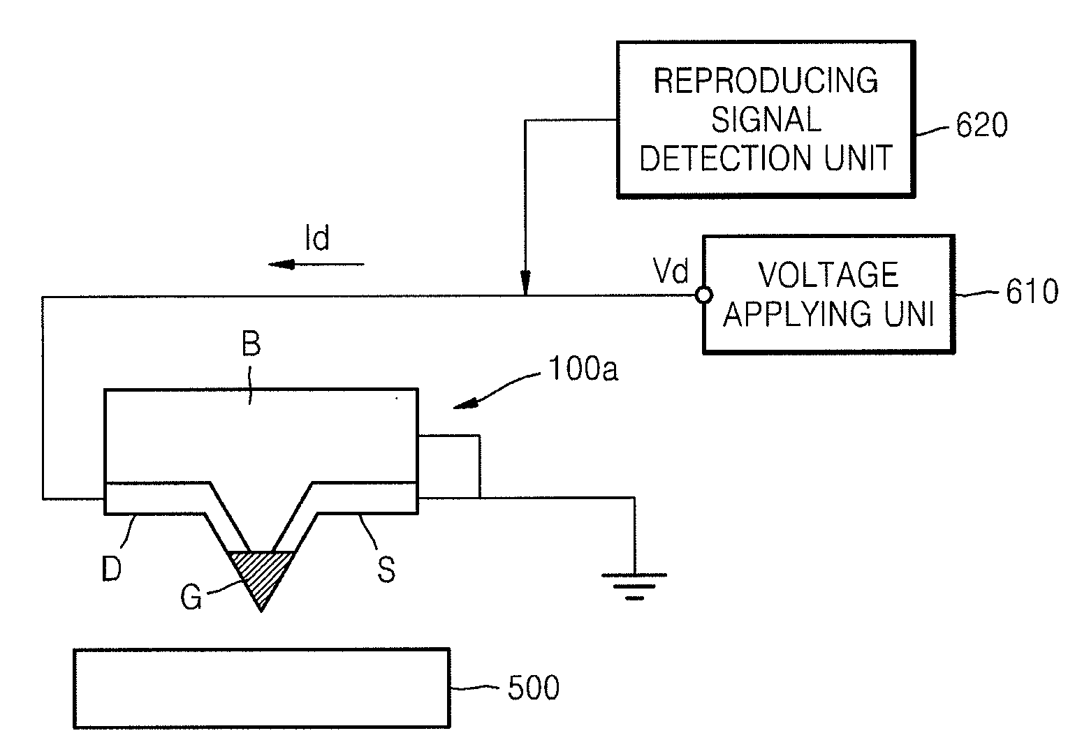
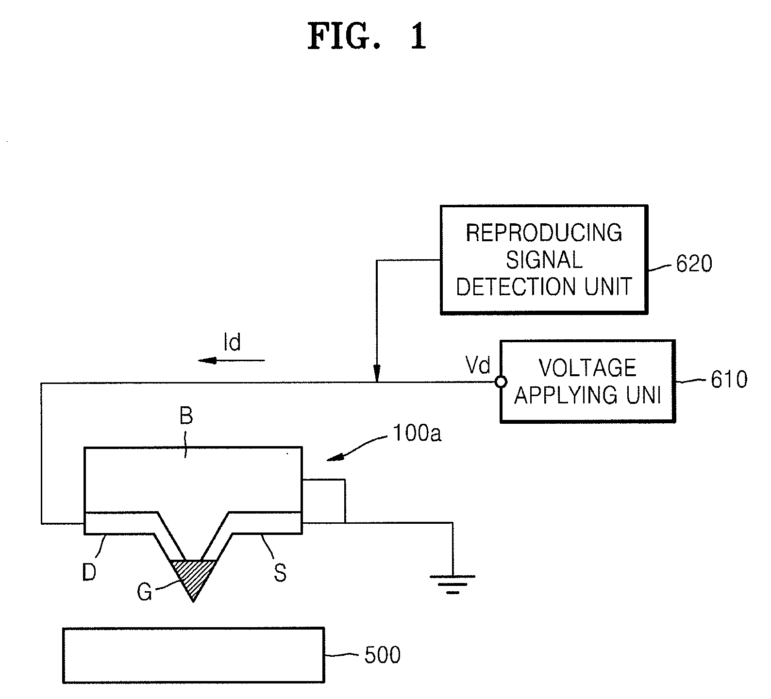
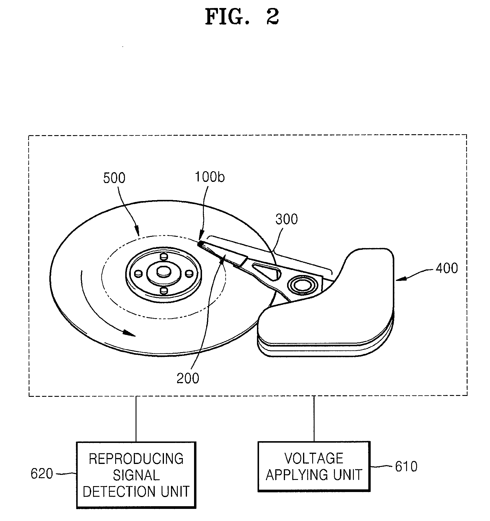
Method of improving sensitivity of electric field sensor, storage apparatus including electric field sensor, and method of reproducing information of the storage apparatus
PatentInactiveUS20090034405A1
Innovation
- The use of an electric field sensor with a resistance region, source, and drain regions, and the integration of negative resistors, such as tunnel diodes connected in series or parallel, to enhance sensitivity by detecting changes in drain current and voltage, allowing for improved read/write capabilities on ferroelectric recording media.

Component in algainn system comprising a tunnel junction
PatentWO2017148476A1
Innovation
- Introducing foreign atoms to create deep imperfections within the space charge zone of the tunnel diode, which generate additional energetic states for improved tunneling probabilities, and using targeted doping with transition metals, carbon, or tin to enhance hole concentrations and reduce effective barrier thickness, while maintaining high reproducibility and charge carrier transport.


Materials Science Advancements for Tunnel Diodes
Recent advancements in materials science have significantly contributed to enhancing tunnel diode functionality in passive devices. The evolution of semiconductor materials has enabled the development of tunnel diodes with improved performance characteristics, including higher peak-to-valley current ratios and faster switching speeds. Traditional germanium-based tunnel diodes have been largely replaced by compound semiconductor materials such as gallium arsenide (GaAs) and indium phosphide (InP), which offer superior electron mobility and tunneling efficiency.
Nanomaterials have emerged as particularly promising for tunnel diode applications. Two-dimensional materials like graphene and transition metal dichalcogenides (TMDs) exhibit exceptional electronic properties that can be leveraged to create tunnel diodes with unprecedented performance metrics. These materials feature atomically thin profiles that facilitate quantum tunneling effects while maintaining structural integrity under various operating conditions.
The integration of heterostructures has revolutionized tunnel diode design by allowing precise control over band alignments and tunneling barriers. By carefully engineering the interface between different semiconductor materials, researchers have achieved enhanced tunneling probabilities and reduced parasitic capacitance. This approach has proven especially valuable for passive device applications where power consumption and response time are critical factors.
Doping techniques have also evolved substantially, enabling more precise control over carrier concentrations in tunnel diode structures. Advanced methods such as delta doping and modulation doping have made it possible to create highly localized regions of elevated carrier density, optimizing the tunneling process without compromising other device parameters. These techniques have been instrumental in addressing the traditional limitations of tunnel diodes in passive circuit applications.
Surface passivation technologies represent another significant advancement, as they mitigate the detrimental effects of surface states on tunnel diode performance. Novel passivation materials and processes have been developed to reduce interface trap densities and prevent unwanted carrier recombination, resulting in more stable and reliable device operation across varying environmental conditions.
The emergence of strain engineering as a design parameter has opened new avenues for tunnel diode optimization. By deliberately introducing mechanical strain into the crystal lattice, researchers can modify the band structure of semiconductor materials to enhance tunneling efficiency. This approach has proven particularly effective in silicon-germanium (SiGe) systems, where strain-induced band modifications significantly improve device characteristics without requiring exotic materials.
Energy Harvesting Applications and Potential
Tunnel diodes, with their unique negative resistance characteristics, present significant opportunities in the field of energy harvesting. These devices can efficiently convert ambient energy sources such as radio frequency (RF) signals, thermal gradients, and mechanical vibrations into usable electrical power. The optimization of tunnel diode functionality in passive energy harvesting systems could revolutionize how we power low-energy devices, particularly in remote or inaccessible locations.
In RF energy harvesting applications, optimized tunnel diodes can significantly improve the conversion efficiency of ambient electromagnetic waves into DC power. This capability is particularly valuable in urban environments where RF signals from cellular networks, Wi-Fi, and broadcasting stations are abundant. Recent studies have demonstrated that properly configured tunnel diode circuits can achieve conversion efficiencies exceeding 70% at specific frequency ranges, substantially outperforming conventional diode-based rectifiers.
Thermal energy harvesting represents another promising application area. By leveraging the quantum tunneling effect across temperature gradients, optimized tunnel diodes can generate electrical power from even small thermal differences. This capability makes them ideal for powering sensors in industrial settings where temperature variations naturally occur, or in wearable devices that can harvest body heat.
The integration of tunnel diodes with mechanical energy harvesters such as piezoelectric materials creates hybrid systems capable of capturing energy from vibrations and movement. These systems show particular promise for infrastructure monitoring applications, where sensors need to operate autonomously for extended periods without battery replacement.
Looking toward future potential, the miniaturization of tunnel diode-based energy harvesters could enable self-powered microelectronic devices and sensors for Internet of Things (IoT) applications. The development of nanoscale tunnel diodes with enhanced negative resistance characteristics could further improve energy conversion efficiencies, potentially enabling a new generation of self-sustaining electronic systems.
Medical implants represent another frontier for tunnel diode energy harvesting applications. Optimized passive devices could potentially harvest energy from bodily functions to power pacemakers, neural stimulators, and monitoring devices, eliminating the need for battery replacement surgeries and extending device lifespans significantly.
As research continues to advance tunnel diode optimization for passive devices, we can anticipate breakthroughs in ultra-low power electronics that operate entirely on harvested energy, contributing to more sustainable technological ecosystems and enabling new applications in remote sensing, environmental monitoring, and distributed intelligence systems.
Unlock deeper insights with PatSnap Eureka Quick Research — get a full tech report to explore trends and direct your research. Try now!
Generate Your Research Report Instantly with AI Agent
Supercharge your innovation with PatSnap Eureka AI Agent Platform!