

OLED Defect Tolerance vs LED: Comparative Fault Analysis
SEP 12, 202510 MIN READ
Generate Your Research Report Instantly with AI Agent
PatSnap Eureka helps you evaluate technical feasibility & market potential.
OLED vs LED Defect Tolerance Background and Objectives
The evolution of display technologies has witnessed significant advancements over the past decades, with Light Emitting Diodes (LEDs) and Organic Light Emitting Diodes (OLEDs) emerging as dominant technologies in various applications. The fundamental difference in their construction and operational principles has led to distinct defect tolerance characteristics, which directly impact manufacturing yields, product reliability, and lifecycle performance.
LED technology, developed in the early 1960s, has matured considerably with robust manufacturing processes that have been refined over decades. These inorganic semiconductor-based devices have traditionally demonstrated high resilience to manufacturing defects and operational stresses. In contrast, OLED technology, which emerged commercially in the late 1990s, utilizes organic compounds that emit light when an electric current passes through them, presenting unique challenges in defect management.
The historical progression of both technologies reveals a consistent trend toward miniaturization and integration density increases, which has amplified the significance of defect tolerance. As pixel densities increase, particularly in high-resolution displays, the impact of individual defective elements becomes more pronounced, necessitating advanced defect management strategies.
Current industry standards for acceptable defect rates differ substantially between LED and OLED technologies. While LED manufacturing has achieved remarkably low defect rates through process optimization, OLED production continues to face challenges related to organic material degradation, encapsulation failures, and pixel uniformity issues. These challenges have direct implications for production costs, device longevity, and market competitiveness.
The primary objective of this comparative fault analysis is to establish a comprehensive understanding of the inherent defect tolerance mechanisms in both LED and OLED technologies. By examining the fundamental physical and chemical properties that influence fault resistance, we aim to identify the critical factors that determine defect propagation, failure modes, and recovery capabilities in each technology.
Furthermore, this analysis seeks to quantify the economic impact of defect tolerance disparities between LEDs and OLEDs across various application domains, including consumer electronics, automotive displays, and industrial systems. Understanding these economic implications is essential for strategic decision-making in technology investment and product development roadmaps.
Additionally, this research aims to forecast the evolution of defect tolerance characteristics as both technologies continue to advance, particularly with the emergence of micro-LED and flexible OLED technologies. Anticipating these trends will provide valuable insights for manufacturing process optimization and quality control strategy development in next-generation display technologies.
Market Demand Analysis for Defect-Tolerant Display Technologies
The display technology market is witnessing a significant shift toward defect-tolerant solutions, driven by increasing consumer demand for higher quality, longer-lasting displays across multiple device categories. Current market research indicates that the global display market is projected to reach $177 billion by 2026, with OLED technology capturing an increasingly substantial portion due to its inherent advantages in defect management compared to traditional LED technologies.
Consumer electronics manufacturers are facing mounting pressure to deliver near-perfect displays while maintaining competitive pricing. This has created a robust demand for display technologies that can maintain performance despite minor manufacturing defects. Smartphone manufacturers particularly value defect tolerance, as screen quality directly impacts consumer satisfaction and brand perception in this premium device segment.
The automotive industry represents another rapidly expanding market for defect-tolerant displays. With the integration of increasingly sophisticated infotainment systems and digital dashboards, automotive manufacturers require displays that maintain functionality and aesthetic appeal throughout the vehicle's lifecycle, often in challenging environmental conditions. Market analysis shows automotive display demand growing at 12% annually, with defect tolerance becoming a key specification in procurement decisions.
Television and large-format display sectors demonstrate similar trends, with consumers showing willingness to pay premium prices for technologies that offer longer lifespans and consistent performance. Retail surveys indicate that visible defects rank among the top three reasons for display product returns, creating significant warranty and customer service costs for manufacturers and retailers alike.
Enterprise and commercial applications present another substantial market segment, where display uptime and reliability directly impact operational efficiency. Digital signage, control room displays, and professional visualization systems all benefit from enhanced defect tolerance, with businesses increasingly factoring total cost of ownership into purchasing decisions rather than focusing solely on initial acquisition costs.
Geographically, North America and Asia-Pacific regions lead in demand for defect-tolerant display technologies, with European markets showing accelerated adoption rates as environmental regulations increasingly favor longer-lasting electronic components to reduce electronic waste. China's domestic market has become particularly significant, with local manufacturers rapidly advancing their defect management capabilities to compete in premium display segments.
Market forecasts suggest that manufacturers demonstrating superior defect tolerance in their display technologies can command price premiums of 15-30% compared to less reliable alternatives. This price elasticity indicates strong consumer and business recognition of the value proposition offered by more robust display technologies, creating substantial revenue opportunities for companies that can effectively address this market need.
Current Technical Challenges in OLED and LED Fault Management
Both OLED and LED technologies face distinct technical challenges in fault management that significantly impact their reliability, performance, and manufacturing yield. OLED displays exhibit a higher sensitivity to defects due to their organic materials and complex multi-layer structure. The primary challenge in OLED fault management is the progressive degradation of organic materials, leading to issues like differential aging and color shift over time. This degradation is accelerated by exposure to oxygen, moisture, and operational heat, requiring sophisticated encapsulation techniques that add complexity to manufacturing processes.
Pixel defects in OLEDs present unique challenges compared to LEDs. When an OLED pixel fails, it typically manifests as a "dead pixel" that remains permanently dark, creating noticeable visual artifacts in high-resolution displays. The interconnected nature of OLED matrices means that single-point failures can potentially affect entire rows or columns, particularly in passive-matrix configurations. This cascading effect significantly complicates fault isolation and management strategies.
LED technology, while more mature, faces its own set of challenges. Thermal management remains a critical issue, as LEDs generate substantial heat during operation that must be efficiently dissipated to prevent accelerated degradation and color shift. The binning process for LEDs—sorting based on brightness and color characteristics—introduces variability that must be compensated for in large displays to ensure visual uniformity.
Manufacturing yield represents a significant economic challenge for both technologies. OLED production suffers from lower yields compared to LEDs, particularly for larger display sizes, driving up costs and limiting market penetration in certain segments. The complex deposition processes for OLED layers are highly sensitive to particulate contamination, requiring cleanroom environments that exceed even semiconductor manufacturing standards in some cases.
Fault detection methodologies differ substantially between the technologies. LED fault detection can often be performed through electrical testing, while OLED defects may require sophisticated optical inspection systems capable of detecting subtle variations in luminance and chromaticity. The development of real-time monitoring systems for OLED degradation remains an active research area with significant technical hurdles.
Repair capabilities represent another divergent challenge. LED arrays typically allow for individual component replacement, while OLED displays generally require replacement of entire modules or panels when defects occur. This fundamental difference impacts maintenance strategies and lifecycle costs for products utilizing these technologies.
The industry continues to develop innovative approaches to address these challenges, including redundant circuit designs, advanced compensation algorithms, and self-healing materials. However, the fundamental physical limitations of organic materials in OLEDs versus inorganic materials in LEDs create persistent differences in their fault tolerance profiles that influence design decisions across multiple application domains.
Comparative Analysis of OLED and LED Fault Tolerance Solutions
01 Pixel compensation techniques for defect tolerance
Various compensation techniques are employed to address pixel defects in OLED and LED displays. These include compensation circuits that detect defective pixels and adjust driving signals to neighboring pixels to maintain display quality. Advanced algorithms can analyze pixel performance in real-time and apply corrective measures to minimize the visual impact of defects, ensuring uniform brightness and color accuracy across the display despite the presence of defective elements.- Pixel compensation techniques for defect tolerance: Various compensation techniques are employed to address pixel defects in OLED and LED displays. These include circuit designs that detect defective pixels and compensate by adjusting current or voltage to neighboring pixels. Advanced algorithms can analyze display performance in real-time and make adjustments to maintain image quality despite defects. These compensation mechanisms help extend the usable life of displays even when some pixels begin to degrade or fail completely.
- Redundant pixel and circuit architectures: Display manufacturers implement redundancy in pixel design and driving circuits to improve defect tolerance. This includes backup sub-pixels, redundant thin-film transistors (TFTs), and duplicate signal lines that can take over when primary components fail. Some designs incorporate parallel circuit paths or multiple emitting elements per pixel to ensure continued operation even if individual components degrade. These redundant architectures significantly improve yield rates in manufacturing and extend the operational lifetime of displays.
- Material and structural innovations for defect prevention: Novel materials and structural designs are developed to inherently reduce defect occurrence in OLED and LED displays. These include improved encapsulation techniques to prevent moisture and oxygen ingress, stress-relieving substrate designs, and more robust electrode materials. Some innovations focus on self-healing materials that can recover from minor damage, or flexible components that better withstand mechanical stress. These material advances significantly reduce the formation of dark spots, pixel shorts, and other common display defects.
- Testing and quality control methods: Advanced testing methodologies are employed during manufacturing to identify and address defects before displays reach consumers. These include automated optical inspection systems, electrical testing of individual pixels, and burn-in procedures to identify weak components. Some manufacturers implement machine learning algorithms to predict potential failure points based on subtle manufacturing variations. These quality control methods help ensure that displays meet defect tolerance specifications and maintain consistent performance.
- Defect masking and image processing techniques: Software-based approaches are used to mask or compensate for visible defects in OLED and LED displays. These include image processing algorithms that can detect defective pixels and adjust surrounding pixels to make defects less noticeable. Some systems dynamically remap content to avoid using known defective areas of the display. Advanced techniques may include content-aware algorithms that analyze the displayed image and apply different compensation strategies depending on the visual content, making defects virtually imperceptible to users.
02 Redundant pixel architectures for improved defect tolerance
Display manufacturers implement redundant pixel designs where backup sub-pixels or transistors are incorporated into the display architecture. If a primary pixel element fails, the system can switch to the redundant component, maintaining display functionality. This approach significantly improves yield rates in manufacturing and extends the operational lifespan of displays by providing fault tolerance against common defect mechanisms in both OLED and LED technologies.Expand Specific Solutions03 Material and structural innovations for defect resistance
Advanced materials and structural designs enhance the inherent defect resistance of OLED and LED displays. These innovations include encapsulation technologies that protect sensitive organic materials from moisture and oxygen, more robust electrode materials that resist cracking and delamination, and novel pixel structures that distribute electrical and thermal stress more evenly. These approaches reduce the likelihood of defect formation during both manufacturing and operation.Expand Specific Solutions04 Testing and quality control systems for defect identification
Sophisticated testing and quality control systems are implemented to identify and categorize display defects before products reach consumers. These systems employ machine vision, electrical testing, and optical analysis to detect various defect types including dead pixels, brightness variations, and color inconsistencies. Early detection allows for either repair of defects during manufacturing or appropriate binning of displays based on defect levels, optimizing yield management.Expand Specific Solutions05 Flexible display technologies with enhanced defect tolerance
Flexible OLED and LED displays incorporate special design features to tolerate mechanical stress-induced defects. These include strain-resistant thin film transistors, elastic interconnect structures, and neutral plane engineering to minimize stress on critical components during bending. Additionally, specialized buffer layers and substrate materials help distribute mechanical forces more evenly, preventing localized defects from forming when the display is flexed or folded repeatedly.Expand Specific Solutions
Key Industry Players in Display Manufacturing and Quality Control
The OLED defect tolerance versus LED comparative fault analysis market is currently in a growth phase, with an estimated market size of $15-20 billion and expanding at 15% annually. The technology maturity landscape shows varying levels of advancement among key players. Industry leaders like Samsung Display and LG Display have achieved high maturity in OLED defect management through significant R&D investments, while BOE Technology is rapidly closing the gap with innovative fault tolerance systems. Traditional LED manufacturers such as Tridonic and Varroc Lighting Systems maintain strong positions in conventional LED reliability engineering. Emerging players like X Display Co. and Cambridge Display Technology are introducing disruptive approaches to defect mitigation. The competitive landscape is characterized by increasing convergence between display and semiconductor technologies, with companies like Himax Technologies and LX Semicon developing integrated solutions addressing both OLED and LED fault tolerance challenges.
BOE Technology Group Co., Ltd.
Technical Solution: BOE has developed a multi-tiered approach to OLED defect tolerance that combines hardware redundancy with software compensation. Their OLED panels feature redundant driving transistors for critical pixel elements, allowing automatic switching to backup circuits when primary components fail. BOE's manufacturing process incorporates high-precision laser repair technology that can address certain types of defects during production, significantly reducing defect rates in finished panels. Their proprietary "Intelligent Pixel Management" system continuously monitors pixel performance and applies compensation algorithms that adjust voltage distribution across the display to minimize the visual impact of any defects. BOE has also implemented advanced thin-film encapsulation techniques that provide superior protection against moisture and oxygen penetration - common causes of OLED degradation and defects. Unlike conventional LED displays that typically require full module replacement when defects occur, BOE's OLED architecture allows for more granular defect management, with many issues addressable through driver-level adjustments rather than hardware replacement.
Strengths: Effective combination of hardware redundancy and software compensation; advanced laser repair capabilities during manufacturing; superior encapsulation technology for defect prevention. Weaknesses: Compensation techniques can increase power consumption; repair technologies add manufacturing complexity; some defect types still require complete panel replacement.
LG Display Co., Ltd.
Technical Solution: LG Display has engineered a comprehensive OLED defect tolerance framework that addresses both manufacturing and operational failures. Their approach incorporates multi-layered redundancy systems where each pixel contains backup TFT circuits that activate when primary circuits fail. LG's proprietary "Pixel Refresh" technology periodically runs diagnostics and applies corrective voltage patterns to prevent permanent image retention and address early-stage pixel degradation. For manufacturing defects, LG employs AI-powered optical inspection systems that can detect sub-micron irregularities and predict potential failure points before they manifest as visible defects. Their OLED panels feature isolated pixel structures that prevent defect propagation - a significant advantage over LED displays where thermal issues in one component can cascade to neighboring elements. LG has also developed compensation algorithms that adjust surrounding pixels' brightness to mask the visual impact of defective pixels, making defects virtually undetectable to users.
Strengths: Advanced AI-based defect prediction and prevention; effective isolation of defects to prevent propagation; sophisticated compensation algorithms for masking unavoidable defects. Weaknesses: Pixel refresh operations can temporarily impact display availability; higher production costs compared to LED; some compensation techniques reduce overall brightness.
Critical Patents and Research in Display Defect Management
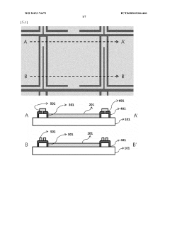
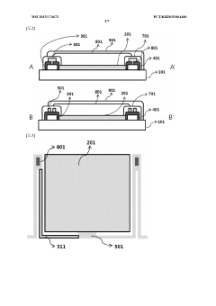
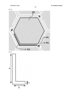
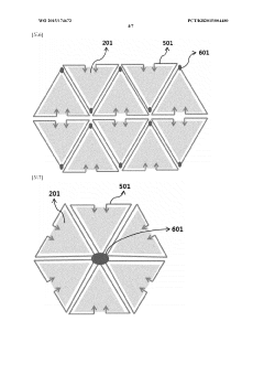
Organic light-emitting device and method for preparing same
PatentWO2015174672A1
Innovation
- The OLED design includes a substrate with spaced conductive units, an auxiliary electrode, and an insulating layer with contact holes, featuring high-resistance regions in the conductive connection parts to prevent current leakage and maintain functionality even with short-circuit defects, by ensuring current flows through defect-free regions.
Organic light emitting device
PatentWO2015163719A1
Innovation
- Incorporating a substrate with a first electrode having two or more conductive units, an auxiliary electrode electrically connected to each conductive unit, and a short-circuit preventing unit with a resistance of 500 Ω or more and 800,000 Ω or less between the auxiliary electrode and the conductive units to prevent short circuits and maintain device functionality.
Manufacturing Process Impact on Display Defect Rates
The manufacturing processes for OLED and LED displays significantly influence their respective defect rates and overall yield. OLED manufacturing involves complex deposition of organic materials in multiple layers, requiring precise vacuum environments and temperature controls. This intricate process inherently creates more opportunities for defects compared to LED manufacturing, which utilizes more established semiconductor fabrication techniques.
In OLED production, the critical thin-film transistor (TFT) backplane fabrication represents a major source of potential defects. Even microscopic particles or slight variations in deposition can lead to dead pixels or subpixels. The organic materials themselves are highly sensitive to oxygen and moisture, necessitating stringent manufacturing conditions that add complexity and increase defect probability.
LED display manufacturing, particularly for mini-LED and micro-LED technologies, benefits from more mature semiconductor processes. The inorganic materials used in LEDs demonstrate greater stability during manufacturing, allowing for higher tolerance to process variations. However, as pixel densities increase in advanced LED displays, manufacturing challenges begin to approach those of OLEDs, particularly in transfer processes for micro-LEDs.
Statistical analysis reveals that OLED manufacturing typically experiences defect rates 1.5-2.5 times higher than comparable LED technologies at similar resolution points. This difference becomes more pronounced as display sizes increase, with large OLED panels showing exponentially higher defect rates due to the statistical probability of defects across larger surface areas.
Manufacturing yield improvements have been significant for both technologies over the past decade. OLED yields have improved from below 50% for early large panels to current industry averages of 70-85%, while LED-based displays typically achieve yields of 85-95%. These improvements stem from enhanced clean room technologies, automated optical inspection systems, and advanced process controls.
The economic impact of these defect rates manifests in production costs. OLED displays typically require more sophisticated defect compensation algorithms and redundancy designs to maintain acceptable yields. In contrast, LED manufacturing can often implement simpler binning and selection processes to manage defects, contributing to more cost-effective production at scale.
Recent innovations in encapsulation technologies and thin-film deposition methods have shown promise in reducing OLED defect rates, potentially narrowing the gap with LED manufacturing yields in future production generations. Meanwhile, as micro-LED manufacturing scales to higher volumes, new transfer-related defects are emerging as significant challenges that may influence the comparative defect analysis between these competing display technologies.
Cost-Benefit Analysis of Defect Management Strategies
When evaluating defect management strategies for OLED versus LED technologies, a comprehensive cost-benefit analysis reveals significant differences in economic implications. OLED manufacturing processes typically incur higher defect rates during production, with pixel failures occurring at approximately 2-5% in standard manufacturing lines. These defects translate to increased production costs, with estimates suggesting that defect management accounts for 15-20% of total OLED manufacturing expenses.
In contrast, LED technology demonstrates greater inherent fault tolerance, with typical defect rates below 1% in mature production environments. This fundamental difference creates a distinct economic landscape when comparing defect management approaches between the two technologies. For LED manufacturers, investments in preventive quality control measures yield higher returns due to the relatively straightforward identification and correction of defects during production.
OLED manufacturers face more complex economic calculations. The implementation of advanced defect compensation algorithms and redundancy systems represents a significant upfront investment, often ranging from $2-5 million for production line upgrades. However, these systems can reduce post-production rejection rates by 30-40%, creating substantial long-term savings that typically achieve ROI within 18-24 months of implementation.
The economic equation is further complicated by market considerations. Premium OLED applications in high-end consumer electronics command price points that can absorb higher production costs, while maintaining strict quality standards. This creates a scenario where extensive defect management investments remain economically viable despite their cost. Conversely, LED applications often compete in more price-sensitive markets where minimizing production costs takes precedence.
Lifecycle considerations also impact the cost-benefit calculation. OLED defects tend to increase over the product lifespan, with pixel degradation accelerating in later usage stages. This creates warranty and reputation costs that must be factored into initial defect management investments. LED technologies demonstrate greater stability over time, reducing the economic impact of long-term defect emergence.
The optimal economic strategy varies significantly based on production scale. Large-volume OLED manufacturers benefit from economies of scale in implementing sophisticated defect management systems, while smaller producers may find the investment prohibitive. This creates market segmentation where different economic approaches to defect tolerance become viable based on production capacity and target market positioning.
Unlock deeper insights with PatSnap Eureka Quick Research — get a full tech report to explore trends and direct your research. Try now!
Generate Your Research Report Instantly with AI Agent
Supercharge your innovation with PatSnap Eureka AI Agent Platform!