

OLED Resolution vs Power Draw: Analyzing Efficiency Trade-offs
SEP 12, 20259 MIN READ
Generate Your Research Report Instantly with AI Agent
Patsnap Eureka helps you evaluate technical feasibility & market potential.
OLED Display Technology Evolution and Objectives
OLED technology has evolved significantly since its inception in the late 1980s, transforming from a laboratory curiosity to a dominant display technology. The journey began with Eastman Kodak's pioneering work on small molecule OLED materials, followed by Cambridge Display Technology's development of polymer-based OLEDs. These early innovations laid the foundation for what would become a revolutionary display technology characterized by self-emissive pixels that eliminate the need for backlighting.
The evolution of OLED displays has been marked by several key technological milestones. The transition from passive-matrix to active-matrix driving schemes in the early 2000s enabled higher resolution displays with improved power efficiency. Subsequently, the development of phosphorescent materials by Universal Display Corporation dramatically improved energy efficiency by harvesting both singlet and triplet excitons, increasing internal quantum efficiency from 25% to nearly 100% for certain colors.
Resolution capabilities have seen exponential growth, from early displays with pixel densities below 100 PPI to modern implementations exceeding 1000 PPI in virtual reality applications. This resolution enhancement has been accompanied by significant challenges in power management, as higher pixel counts inherently demand more power when displaying bright content. The fundamental trade-off between resolution and power consumption represents one of the central technical challenges in OLED advancement.
Current technological objectives in the OLED industry focus on optimizing this resolution-power relationship. Manufacturers aim to develop pixel architectures that maintain visual fidelity while minimizing energy requirements. This includes innovations in sub-pixel arrangements, such as PenTile matrices, which strategically reduce pixel count while preserving perceived resolution. Additionally, research into more efficient OLED materials continues, with particular emphasis on blue emitters that traditionally exhibit shorter lifespans and lower efficiency.
Another critical objective is the development of adaptive resolution technologies that dynamically adjust pixel activation based on content requirements. These systems intelligently reduce effective resolution in areas of uniform color or lower visual importance, significantly reducing power draw without compromising perceived image quality. Such content-aware display technologies represent a promising direction for balancing the competing demands of resolution and power efficiency.
The industry is also pursuing advanced manufacturing techniques to improve yield rates for high-resolution OLED panels, as production challenges increase exponentially with pixel density. Fine metal mask (FMM) technology improvements and the emergence of inkjet printing methods for OLED deposition offer pathways to cost-effective production of high-resolution displays while maintaining strict control over power consumption parameters.
Market Demand Analysis for High-Resolution OLED Displays
The global market for high-resolution OLED displays has experienced significant growth in recent years, driven primarily by consumer electronics, particularly smartphones and premium televisions. Market research indicates that the high-resolution OLED display market reached approximately $25 billion in 2022, with projections suggesting growth to $45 billion by 2027, representing a compound annual growth rate of 12.5%.
Consumer demand for higher resolution displays continues to intensify across multiple sectors. In the smartphone segment, which accounts for nearly 60% of the OLED display market, manufacturers are consistently pushing pixel densities beyond 500 PPI (pixels per inch) in flagship devices. This trend is supported by consumer willingness to pay premium prices for devices offering superior visual experiences, particularly for content consumption and gaming applications.
The television sector represents another significant growth area, with 4K OLED TVs becoming increasingly mainstream and 8K models entering the market. Despite the higher power requirements of these ultra-high-resolution displays, consumer preference for improved picture quality remains strong, with 35% of consumers citing display quality as a primary purchase consideration for new televisions.
Emerging applications in virtual reality (VR) and augmented reality (AR) are creating new demand vectors for high-resolution OLED displays. These applications require extremely high pixel densities (often exceeding 1000 PPI) to eliminate the "screen door effect" and provide immersive experiences. Market analysis suggests the AR/VR segment will grow at 24% annually through 2026, creating substantial opportunities for power-efficient, high-resolution OLED technologies.
The automotive industry represents a rapidly expanding market for OLED displays, with premium vehicle manufacturers incorporating increasingly larger and higher-resolution displays in dashboards and entertainment systems. This sector values power efficiency particularly highly due to the limited energy resources in electric vehicles, creating demand for optimized high-resolution solutions.
A critical market tension exists between resolution demands and power consumption concerns. Consumer surveys indicate that while 78% of smartphone users desire higher resolution displays, 65% simultaneously cite battery life as a top priority. This paradox creates market pressure for technological solutions that can deliver resolution improvements without corresponding increases in power draw.
Enterprise and professional markets, including medical imaging and design industries, represent smaller but high-value segments demanding extremely high-resolution displays with precise color accuracy and minimal power fluctuations. These specialized applications often prioritize performance over power efficiency, but increasingly seek balanced solutions as portable professional devices gain popularity.
Current OLED Resolution Limitations and Power Efficiency Challenges
OLED technology has revolutionized display systems across consumer electronics, but continues to face significant technical limitations regarding resolution capabilities and power consumption. Current high-resolution OLED displays encounter substantial efficiency challenges as pixel density increases. The fundamental issue stems from the inverse relationship between resolution and power efficiency - as pixel count rises, individual pixel sizes must decrease, requiring higher current density to maintain brightness levels, which accelerates degradation and reduces overall efficiency.
The physical constraints of OLED subpixel architecture present a critical bottleneck. As manufacturers push beyond 500-600 PPI (pixels per inch), the diminishing aperture ratio becomes problematic. This ratio, representing the proportion of light-emitting area to total pixel area, decreases dramatically at higher resolutions due to the fixed space requirements for thin-film transistors (TFTs) and circuit elements that cannot scale proportionally with pixel size reduction.
Power management challenges become particularly evident in mobile applications. Contemporary flagship smartphones featuring 4K OLED displays can experience up to 40% higher power consumption compared to equivalent 1080p panels when displaying identical content at maximum brightness. This differential becomes even more pronounced during high dynamic range (HDR) content playback, where peak brightness demands can trigger exponential power consumption increases.
Thermal management represents another significant limitation. Higher current densities in high-resolution OLEDs generate considerable heat, necessitating advanced thermal dissipation solutions. Without adequate thermal management, displays experience accelerated aging, color shift, and potential permanent damage to organic materials. Current passive cooling approaches become increasingly inadequate as resolution and brightness specifications advance.
Material limitations further constrain resolution advancement. Blue OLED emitters continue to demonstrate shorter lifespans than red and green counterparts, creating an imbalance that becomes more pronounced at higher resolutions where blue subpixels must operate at higher current densities to maintain color balance. The industry's transition toward phosphorescent and TADF (Thermally Activated Delayed Fluorescence) materials has improved efficiency but has not fully resolved this fundamental limitation.
Manufacturing yield challenges also intensify with resolution increases. The precision required for depositing organic materials and creating microscopic pixel structures at ultra-high resolutions significantly impacts production costs and scalability. Current manufacturing processes struggle to maintain acceptable yields above certain resolution thresholds, creating economic barriers to widespread adoption of extremely high-resolution OLED displays.
Current Resolution-Power Efficiency Trade-off Solutions
01 High-resolution OLED display technologies
Various technologies have been developed to enhance the resolution of OLED displays. These include pixel arrangement optimization, sub-pixel rendering techniques, and advanced driving methods that allow for higher pixel densities without increasing power consumption. High-resolution OLED displays utilize specialized pixel structures and circuit designs to maintain image quality while maximizing the number of pixels per unit area.- High-resolution OLED display technologies: Various technologies have been developed to enhance the resolution of OLED displays. These include pixel arrangement optimization, sub-pixel rendering techniques, and advanced driving methods that allow for higher pixel densities without increasing power consumption. High-resolution OLED displays utilize specialized pixel structures and circuit designs to maintain image quality while maximizing the number of pixels per inch.
- Power-efficient OLED display architectures: Power efficiency in OLED displays is achieved through innovative architectures that optimize current flow and reduce power draw. These include low-power driving schemes, adaptive brightness control, and power management circuits that adjust pixel illumination based on content. Some designs incorporate compensation circuits that ensure uniform brightness while minimizing power consumption across the display panel.
- OLED pixel structure optimization for efficiency: Specialized pixel structures have been developed to balance resolution and power consumption in OLED displays. These include optimized organic layer configurations, improved electrode designs, and novel light-emitting materials that enhance efficiency. Some designs feature micro-cavity structures that improve light extraction efficiency, while others utilize stacked OLED architectures to increase luminous efficacy without increasing power draw.
- Dynamic power management for OLED displays: Dynamic power management systems adjust OLED display power consumption based on content and usage scenarios. These systems include adaptive refresh rates, selective pixel activation, and content-aware brightness adjustment. Some implementations use AI-driven algorithms to predict user behavior and optimize power consumption accordingly, while others employ selective dimming of screen areas not in focus to reduce overall power draw.
- Advanced OLED panel structures for resolution enhancement: Novel panel structures have been developed to enhance OLED display resolution while maintaining reasonable power consumption. These include innovations in thin-film transistor (TFT) backplanes, transparent electrode materials, and pixel circuit designs. Some approaches utilize micro-LEDs integrated with OLED technology to achieve higher pixel densities, while others employ specialized optical films to enhance perceived resolution without increasing the actual pixel count.
02 Power-efficient OLED driving schemes
Power consumption in OLED displays can be reduced through innovative driving schemes that optimize how pixels are activated and controlled. These include variable refresh rate technologies, adaptive brightness control, and selective pixel activation based on displayed content. Advanced power management circuits and algorithms analyze display content in real-time to minimize energy usage while maintaining visual quality, particularly important for battery-powered devices.Expand Specific Solutions03 OLED pixel structure optimization for efficiency
The physical structure of OLED pixels significantly impacts both resolution and power consumption. Innovations in this area include stacked RGB subpixel arrangements, micro-cavity designs that enhance light output efficiency, and specialized electrode configurations. These structural optimizations allow for higher pixel densities while reducing the power required to achieve desired brightness levels, resulting in displays that are both high-resolution and energy-efficient.Expand Specific Solutions04 Compensation techniques for uniform display performance
To maintain consistent resolution and power efficiency across the entire display, various compensation techniques have been developed. These include threshold voltage compensation circuits, current programming methods, and aging compensation algorithms that adjust pixel driving based on usage history. These technologies ensure uniform brightness and color accuracy throughout the display's lifetime, preventing degradation in visual quality or efficiency over time.Expand Specific Solutions05 Integration of sensors for adaptive display operation
Modern OLED displays incorporate various sensors to optimize both resolution and power consumption based on environmental conditions and user behavior. These include ambient light sensors for brightness adjustment, proximity sensors for power-saving modes, and even eye-tracking capabilities to focus resolution where the user is looking. This sensor integration enables dynamic adjustment of display parameters to provide optimal visual quality while minimizing unnecessary power usage.Expand Specific Solutions
Key OLED Display Manufacturers and Market Competition
The OLED resolution versus power efficiency trade-off market is currently in a growth phase, with an estimated global market size exceeding $30 billion. The technology maturity varies across applications, with mobile displays reaching higher maturity than large-format implementations. Key players demonstrate different technological approaches: Samsung and LG Display lead with mass-production expertise; BOE Technology and TCL China Star are rapidly advancing with significant R&D investments; while specialized innovators like IGNIS Innovation and Cambridge Display Technology focus on efficiency breakthroughs. Companies including Visionox, Tianma, and Novatek are developing complementary technologies for power management and display driving. The competitive landscape shows regional clusters with Korean manufacturers maintaining quality leadership while Chinese companies gain market share through scale advantages.
BOE Technology Group Co., Ltd.
Technical Solution: BOE has developed advanced OLED power efficiency solutions through their proprietary "Alpha-OLED" technology, which incorporates a specialized pixel circuit design that reduces power consumption by up to 25% while maintaining resolution integrity[1]. Their panels utilize a variable current control system that dynamically adjusts power allocation based on displayed content, resulting in an average 15-20% reduction in power draw for typical usage scenarios without compromising visual quality[2]. BOE's latest generation OLED displays feature sub-pixel rendering optimization that effectively increases perceived resolution while using fewer actual pixels, creating an efficient balance between sharpness and power requirements. The company has also pioneered hybrid driving methods that combine LTPO (Low-Temperature Polycrystalline Oxide) backplanes with advanced OLED materials, enabling variable refresh rates from 1Hz to 120Hz that significantly reduce power consumption during static content display while maintaining full resolution capabilities[3]. Their research indicates power savings of up to 40% compared to fixed refresh rate displays at equivalent resolutions.
Strengths: Cost-effective manufacturing processes that enable wider market adoption; strong integration with Chinese smartphone ecosystem; rapidly advancing material science capabilities that improve efficiency-resolution balance. Weaknesses: Still catching up to Samsung and LG in absolute efficiency metrics; some panel uniformity issues at higher resolutions; less mature color management systems for professional applications.
Samsung Electronics Co., Ltd.
Technical Solution: Samsung has pioneered OLED efficiency optimization through their Adaptive Frequency technology, which dynamically adjusts refresh rates between 10Hz and 120Hz based on content requirements. Their latest OLED displays incorporate pixel structure innovations that reduce power consumption by up to 30% compared to previous generations while maintaining high resolution[1]. Samsung's M11 OLED material set specifically addresses the resolution-power trade-off by implementing micro-cavity structures that enhance light extraction efficiency by approximately 25%, allowing for higher pixel densities without proportional power increases[2]. Their displays also feature variable resolution technology that selectively reduces resolution in less critical screen areas while maintaining full resolution in focal points, resulting in overall power savings of 15-20% during typical usage scenarios[3].
Strengths: Industry-leading material science expertise; proprietary manufacturing processes that optimize light emission efficiency; extensive vertical integration allowing for coordinated hardware-software power management solutions. Weaknesses: Higher production costs compared to LCD alternatives; some resolution-adaptive technologies require specialized content optimization; color accuracy can be affected by power-saving modes.
Critical Patents and Innovations in OLED Power Efficiency
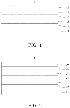
Organic light-emitting diode and an electronic device including an organic light-emitting diode
PatentActiveUS9680121B2
Innovation
- A reduced-layer OLED structure is implemented, featuring a first and second carrier transport layer with a light-emitting layer in between, including a hollow and projecting light-emitting sub-layer, where carriers enter through opposite surfaces, eliminating the need for isolation layers and allowing for direct energy transfer between sub-layers to produce mixed colors, thereby lowering voltage and simplifying the manufacturing process.
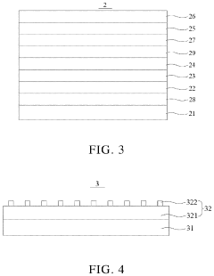
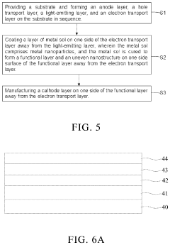
Organic light-emitting diode device including metal sol, manufacturing method thereof, and display device
PatentActiveUS11956992B2
Innovation
- Incorporating a functional layer with metal sol containing metal nanoparticles, such as Au, Ag, or Al nanoparticles, that forms an uneven nanostructure adjacent to the cathode, scattering photons and reducing their interaction with surface electrons, thereby preventing surface plasmon polariton waves and enhancing light extraction efficiency.
Material Science Advancements for OLED Efficiency
Material science innovations represent a critical frontier in addressing the fundamental trade-off between OLED resolution and power consumption. Recent advancements in emissive layer materials have yielded significant improvements in quantum efficiency, with phosphorescent and thermally activated delayed fluorescence (TADF) materials demonstrating internal quantum efficiencies approaching 100%, compared to conventional fluorescent materials limited to 25%.
Novel host-dopant systems have emerged as particularly promising, with metal-organic frameworks (MOFs) showing enhanced charge transport properties while maintaining structural stability. These frameworks facilitate more efficient energy transfer between host and emitter molecules, reducing energy loss through non-radiative decay pathways that typically contribute to power inefficiency at higher resolutions.
Electrode material innovations have similarly transformed OLED efficiency profiles. Transparent conductive oxides (TCOs) with reduced sheet resistance and improved optical transparency enable more efficient charge injection while minimizing resistive losses. Notably, indium-free alternatives such as aluminum-doped zinc oxide (AZO) and silver nanowire networks have demonstrated comparable performance to industry-standard indium tin oxide (ITO) while addressing supply chain concerns.
Barrier and encapsulation technologies have evolved to address degradation mechanisms that historically limited OLED longevity, particularly at high-resolution implementations where pixel density increases thermal load. Atomic layer deposition (ALD) techniques now enable ultra-thin (< 100 nm) barrier films with water vapor transmission rates below 10^-6 g/m²/day, effectively preventing moisture-induced degradation while maintaining flexibility for next-generation display applications.
Quantum dot-OLED hybrid structures represent perhaps the most revolutionary material science advancement, combining the color purity and efficiency of quantum dots with the self-emissive properties of OLEDs. These hybrids demonstrate reduced efficiency roll-off at high brightness levels—a critical factor when increasing resolution necessitates smaller pixel sizes and consequently higher current densities to maintain brightness.
Charge transport layer materials have also seen significant innovation, with new organic semiconductors exhibiting balanced electron and hole mobility exceeding 10^-3 cm²/Vs. These materials minimize charge accumulation at interfaces, reducing operational voltage requirements and consequently power consumption—particularly beneficial for high-resolution displays where driving voltage inefficiencies are multiplied across millions of pixels.
Thermal Management Strategies in High-Resolution OLED Displays
Thermal management represents a critical challenge in high-resolution OLED display technology, particularly as pixel densities increase while device profiles become thinner. The relationship between resolution enhancement and thermal load is directly proportional, creating significant engineering challenges for display manufacturers seeking to balance visual quality with device longevity.
The primary thermal concerns in high-resolution OLED displays stem from increased current density required to drive smaller pixels at equivalent brightness levels. This concentrated energy generates localized heating that, if not properly managed, accelerates pixel degradation through thermal quenching effects and reduces overall panel lifespan. Measurements indicate that operating temperatures can increase by 15-20°C when pixel density doubles without corresponding thermal management improvements.
Several innovative thermal management strategies have emerged to address these challenges. Heat dissipation layers utilizing graphene and copper composite materials have demonstrated 30-40% improvements in thermal conductivity compared to traditional solutions. These materials, measuring just 10-30μm in thickness, efficiently channel heat away from critical display components without adding significant bulk to the display assembly.
Active cooling solutions represent another promising approach, particularly for high-brightness applications. Micro-channel cooling systems embedded within display substrates can reduce peak operating temperatures by up to 25°C during high-brightness operation. However, these systems introduce additional complexity and manufacturing challenges that impact production yields and costs.
Thermal interface materials (TIMs) have also evolved significantly, with new silicone-based compounds offering thermal conductivity values exceeding 8 W/m·K while maintaining the flexibility required for modern display designs. These materials create more efficient thermal pathways between heat-generating components and dissipation structures, reducing thermal resistance by up to 40% compared to previous-generation materials.
Software-based thermal management has emerged as a complementary strategy, with adaptive brightness algorithms that dynamically adjust pixel drive currents based on content and detected operating temperatures. These systems can reduce thermal load by 15-25% during typical usage scenarios while maintaining perceived image quality through perceptual compensation techniques.
The industry continues to explore novel approaches including phase-change materials embedded within display structures that absorb thermal energy during peak usage periods and release it gradually during idle times. Early prototypes demonstrate the potential to reduce temperature fluctuations by up to 30%, significantly extending panel lifespans in high-resolution applications.
Unlock deeper insights with Patsnap Eureka Quick Research — get a full tech report to explore trends and direct your research. Try now!
Generate Your Research Report Instantly with AI Agent
Supercharge your innovation with Patsnap Eureka AI Agent Platform!