

Optimizing Encapsulation Layers for OLED Device Durability
SEP 12, 20259 MIN READ
Generate Your Research Report Instantly with AI Agent
Patsnap Eureka helps you evaluate technical feasibility & market potential.
OLED Encapsulation Technology Background and Objectives
Organic Light-Emitting Diode (OLED) technology has revolutionized display and lighting industries since its commercial introduction in the late 1990s. The evolution of OLED technology has been marked by significant improvements in efficiency, color reproduction, and form factor flexibility. However, device longevity remains a critical challenge due to the inherent sensitivity of organic materials to environmental factors, particularly oxygen and moisture.
The encapsulation layer serves as a protective barrier against these environmental degradation factors, making it a cornerstone of OLED device durability. Early encapsulation techniques relied on glass-to-glass sealing with desiccants, which provided adequate protection but limited the potential for flexible applications. The industry has since witnessed a paradigm shift toward thin-film encapsulation (TFE) technologies, enabling the development of flexible and foldable OLED displays.
Current technological trends indicate a growing emphasis on multi-layer approaches that combine inorganic and organic materials to create effective moisture and oxygen barriers while maintaining flexibility. Atomic Layer Deposition (ALD) has emerged as a promising technique for creating ultra-thin, highly conformal barrier layers with excellent impermeability characteristics. Concurrently, advances in organic-inorganic hybrid materials are addressing the mechanical stress issues inherent in purely inorganic encapsulation solutions.
The primary technical objective of OLED encapsulation research is to achieve a Water Vapor Transmission Rate (WVTR) below 10^-6 g/m²/day and an Oxygen Transmission Rate (OTR) below 10^-5 cc/m²/day, which are considered threshold values for ensuring long-term OLED device stability. Additionally, encapsulation solutions must maintain these barrier properties while accommodating mechanical flexibility for next-generation applications.
Secondary objectives include reducing production costs and complexity, as current high-performance encapsulation methods often involve expensive equipment and time-consuming processes. The industry is also pursuing environmentally sustainable encapsulation materials and processes to align with global sustainability initiatives and regulations.
The convergence of nanotechnology, materials science, and advanced manufacturing techniques is expected to drive the next wave of innovations in OLED encapsulation. Emerging approaches such as graphene-based barriers, metal-organic frameworks (MOFs), and self-healing polymers represent promising research directions that could potentially address current limitations in barrier performance, flexibility, and manufacturing scalability.
As OLED technology continues to expand into new application domains including automotive displays, wearable devices, and architectural lighting, the demands on encapsulation technology will further diversify, necessitating application-specific solutions that balance performance requirements with practical constraints.
Market Analysis for Durable OLED Devices
The global OLED (Organic Light Emitting Diode) market continues to experience robust growth, with a market value reaching $48.5 billion in 2022 and projected to surpass $72.8 billion by 2026. This growth is primarily driven by increasing adoption in smartphones, televisions, and emerging applications such as automotive displays and wearable devices. However, device durability remains a critical factor influencing market expansion and consumer satisfaction.
Consumer research indicates that device longevity ranks among the top three purchasing considerations for premium electronic products. Surveys show that 78% of consumers expect OLED displays to maintain optimal performance for at least 3-5 years, highlighting the importance of effective encapsulation technologies that protect against environmental degradation.
The market for encapsulation materials specifically designed for OLED protection is growing at a compound annual growth rate of 16.7%, outpacing the overall OLED market growth. This acceleration reflects manufacturers' recognition that enhanced durability directly correlates with reduced warranty claims and strengthened brand reputation. Companies investing in superior encapsulation technologies report up to 27% lower return rates compared to industry averages.
Regional market analysis reveals varying consumer expectations and regulatory landscapes. Asian markets, particularly South Korea, Japan, and China, dominate OLED production with 83% of global manufacturing capacity. However, North American and European consumers demonstrate higher willingness to pay premium prices for devices with extended longevity guarantees, creating market opportunities for durability-focused innovations.
Industry forecasts suggest that improvements in OLED durability could unlock significant market expansion in previously resistant sectors. The automotive industry, for instance, has stringent requirements for display longevity under extreme temperature and humidity conditions. Achieving automotive-grade durability standards could open a potential $5.3 billion market segment by 2025.
Competitive analysis indicates that manufacturers who have successfully addressed durability concerns through advanced encapsulation technologies command price premiums averaging 15-22% over comparable products with standard protection. This price elasticity demonstrates strong market validation for investments in durability-enhancing technologies.
The healthcare and industrial display markets represent emerging opportunities, with combined potential reaching $3.7 billion by 2024. These sectors demand exceptional reliability under challenging operating conditions, making advanced encapsulation solutions a prerequisite for market entry and competitive differentiation.
Current Encapsulation Techniques and Barriers
The encapsulation layer serves as a critical barrier against environmental factors that degrade OLED device performance. Current encapsulation techniques can be broadly categorized into three main approaches: glass-based rigid encapsulation, thin-film encapsulation (TFE), and hybrid solutions combining multiple technologies.
Glass-based encapsulation, the earliest and most established technique, utilizes glass substrates sealed with UV-curable epoxy resins. This method provides excellent barrier properties with water vapor transmission rates (WVTR) below 10^-6 g/m²/day, significantly extending device lifetimes. However, its rigidity limits application in flexible displays and increases overall device thickness and weight.
Thin-film encapsulation has emerged as the dominant solution for flexible OLED applications. This approach typically employs alternating layers of inorganic and organic materials. Inorganic layers (commonly Al₂O₃, SiO₂, or SiNₓ) provide excellent barrier properties but are prone to defects and microcracking under mechanical stress. Organic layers (typically polymers like parylene or polyacrylate) offer flexibility and defect-filling capabilities but have inferior barrier properties.
The multi-layer approach in TFE creates a tortuous path for moisture and oxygen penetration, significantly enhancing barrier performance. State-of-the-art TFE systems can achieve WVTR values approaching 10^-6 g/m²/day while maintaining flexibility. Atomic Layer Deposition (ALD) has become the preferred deposition method for inorganic layers due to its ability to create highly conformal, pinhole-free films at relatively low temperatures.
Hybrid encapsulation combines thin-film technologies with additional protective elements. One prominent example is the use of thin-film barriers with edge sealants to address lateral diffusion of contaminants. Another approach incorporates getter materials within the encapsulation structure to actively absorb moisture and oxygen that penetrate the barrier layers.
Despite significant advancements, current encapsulation technologies face several challenges. These include achieving consistent ultra-high barrier performance at scale, maintaining barrier integrity during mechanical deformation, and balancing manufacturing costs with performance requirements. The trade-off between flexibility and barrier properties remains a fundamental challenge, particularly for applications requiring extreme bending radii.
Manufacturing scalability presents another significant barrier, as techniques like ALD require precise process control and relatively long cycle times. Additionally, the industry lacks standardized testing protocols for ultra-barrier films, making performance comparisons between different solutions challenging.
State-of-the-Art Encapsulation Layer Architectures
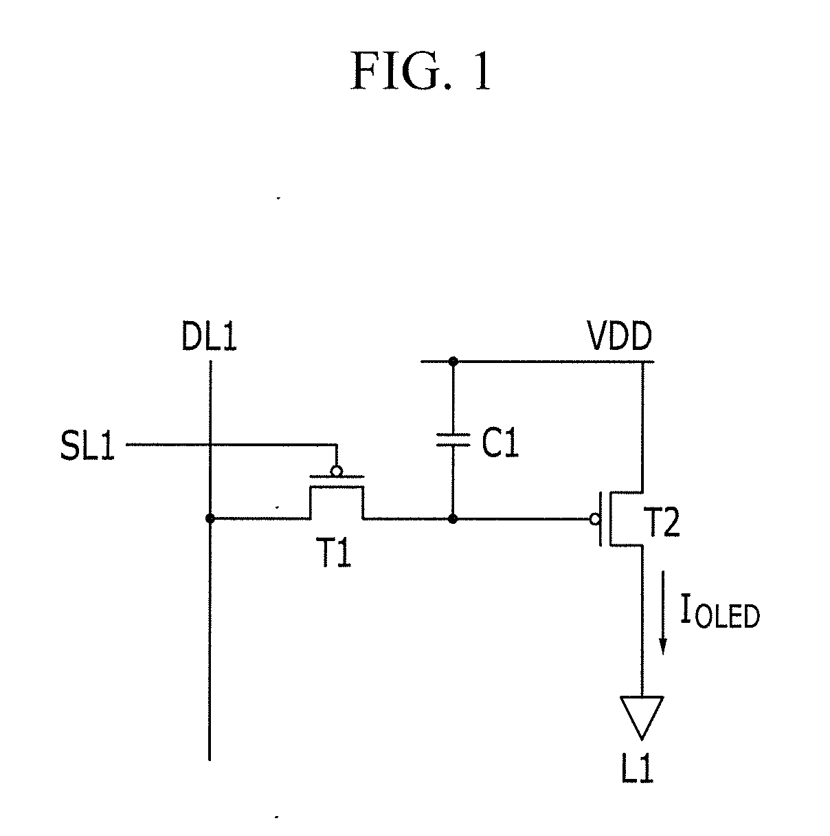
01 Multi-layer encapsulation structures
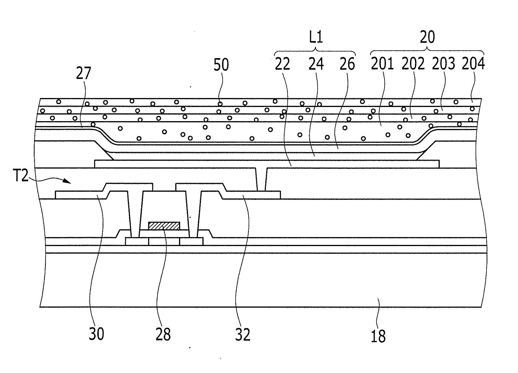
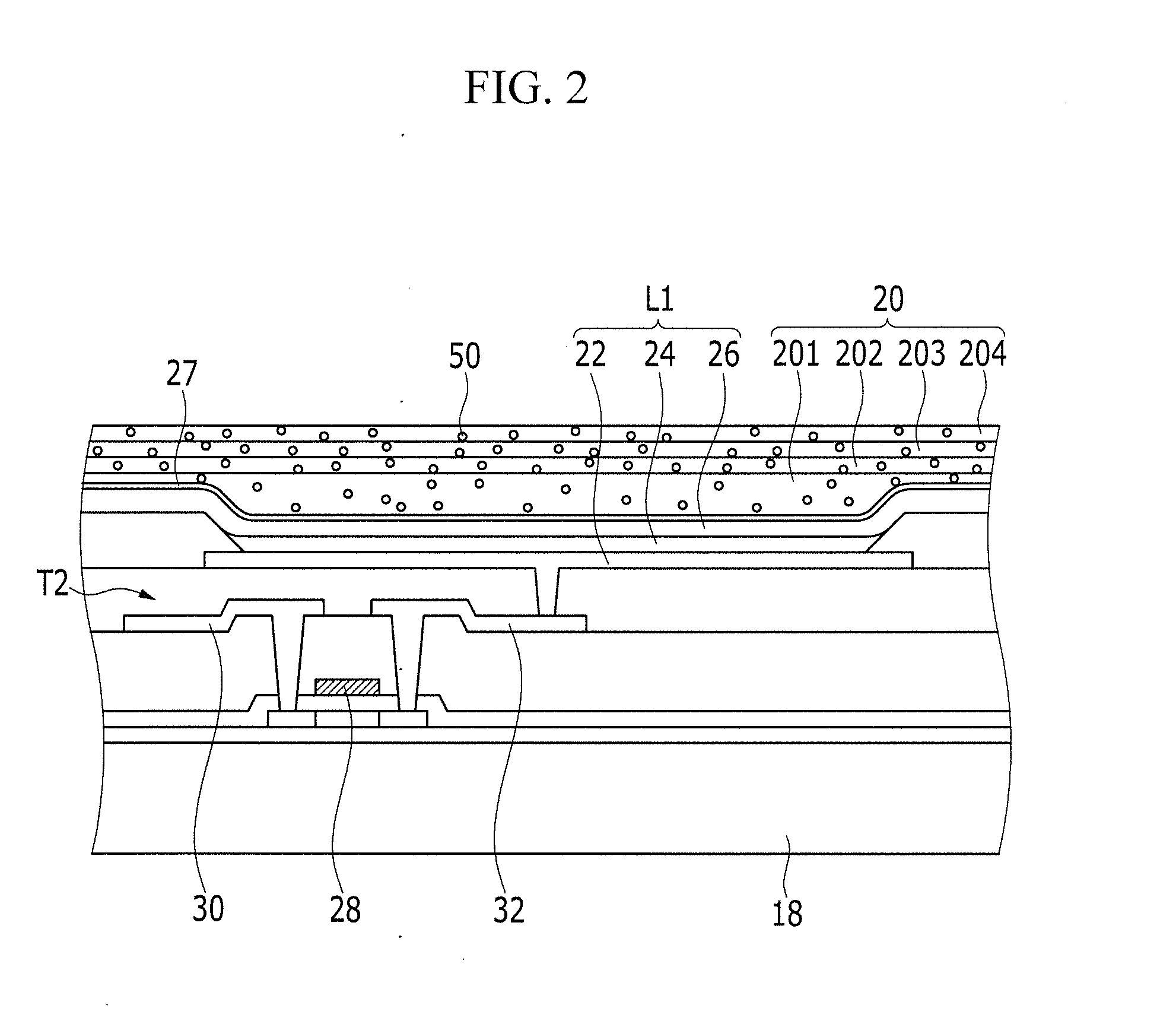
Multi-layer encapsulation structures provide enhanced protection for OLEDs against moisture and oxygen penetration. These structures typically consist of alternating inorganic and organic layers, where inorganic layers act as moisture barriers while organic layers provide flexibility and stress relief. This combination effectively prevents degradation of OLED materials and extends device lifetime. The multi-layer approach allows for thinner overall encapsulation while maintaining high barrier properties.- Multi-layer encapsulation structures: Multi-layer encapsulation structures provide enhanced protection for OLEDs against moisture and oxygen penetration. These structures typically consist of alternating inorganic and organic layers, where inorganic layers act as moisture barriers while organic layers provide flexibility and stress relief. The combination of different materials with complementary properties creates a tortuous path for moisture diffusion, significantly improving device lifetime and durability under various environmental conditions.
- Atomic layer deposition techniques: Atomic layer deposition (ALD) is a key technique for creating high-quality, conformal encapsulation layers for OLEDs. This method allows for precise control over film thickness at the atomic level, resulting in ultra-thin, pinhole-free barrier films. ALD-deposited layers, particularly aluminum oxide and other metal oxides, provide excellent moisture barrier properties while maintaining transparency, which is crucial for maintaining the optical performance of the OLED device.
- Hybrid organic-inorganic encapsulation: Hybrid encapsulation approaches combine organic materials (such as polymers or resins) with inorganic barrier layers to optimize OLED protection. The organic components provide flexibility and crack resistance, while inorganic materials offer superior barrier properties against moisture and oxygen. These hybrid structures can self-heal minor defects and accommodate mechanical stress during device operation, significantly extending OLED lifetime while maintaining device flexibility for applications in foldable or flexible displays.
- Edge sealing technologies: Edge sealing technologies focus on protecting the vulnerable perimeter of OLED devices where moisture and oxygen can easily penetrate. These methods include specialized edge sealants, extended barrier layers, and peripheral encapsulation structures that create a complete hermetic seal around the active area of the device. Effective edge sealing prevents lateral diffusion of harmful elements into the OLED structure, addressing a critical failure mode and significantly improving overall device durability and operational lifetime.
- Thin-film encapsulation with nanoparticles: Incorporating nanoparticles into thin-film encapsulation layers enhances barrier properties and mechanical stability of OLED protective structures. Nanoparticles such as silica, alumina, or metal oxides can fill defects in barrier films, create tortuous diffusion paths for water molecules, and reinforce the mechanical properties of the encapsulation layer. This approach results in improved water vapor transmission rates and better resistance to mechanical stress, extending OLED lifetime while maintaining optical transparency of the encapsulation structure.
02 Inorganic barrier materials
Inorganic materials such as silicon nitride, aluminum oxide, and silicon oxide are commonly used in OLED encapsulation layers due to their excellent barrier properties against moisture and oxygen. These materials can be deposited using various techniques including atomic layer deposition (ALD), chemical vapor deposition (CVD), and sputtering. Inorganic layers provide high density barriers that significantly reduce permeation rates of harmful substances, thereby improving OLED durability and operational lifetime.Expand Specific Solutions03 Hybrid organic-inorganic encapsulation
Hybrid encapsulation systems combine organic and inorganic materials to leverage the advantages of both. Organic materials provide flexibility, stress relief, and planarization, while inorganic materials offer superior barrier properties. This hybrid approach helps mitigate mechanical stress during device operation and thermal cycling, reducing the risk of cracking or delamination. The organic layers can also fill defects in inorganic layers, creating a more comprehensive barrier system that enhances OLED durability.Expand Specific Solutions04 Edge sealing techniques
Edge sealing is critical for preventing lateral moisture and oxygen ingress in OLED devices. Various techniques include frit glass sealing, epoxy-based sealants, and advanced edge encapsulation structures. These methods create a hermetic seal around the perimeter of the device, effectively blocking pathways for contaminants. Proper edge sealing complements the top and bottom encapsulation layers, creating a complete protection system that significantly improves device longevity and reliability under various environmental conditions.Expand Specific Solutions05 Advanced deposition techniques
Advanced deposition methods such as atomic layer deposition (ALD), plasma-enhanced chemical vapor deposition (PECVD), and roll-to-roll processing enable the creation of high-quality encapsulation layers with minimal defects. These techniques allow for precise control over layer thickness, composition, and uniformity, resulting in superior barrier performance. Low-temperature deposition processes have also been developed to accommodate temperature-sensitive OLED materials and flexible substrates, expanding the range of possible applications while maintaining excellent encapsulation properties.Expand Specific Solutions
Leading Companies in OLED Encapsulation Solutions
The OLED encapsulation layer optimization market is currently in a growth phase, with increasing demand driven by the expanding OLED display industry. The global market size is projected to reach significant value as OLED technology continues to penetrate consumer electronics, automotive, and lighting sectors. From a technical maturity perspective, the field shows varied development levels among key players. Companies like LG Chem and BOE Technology have established advanced encapsulation technologies, while Applied Materials provides critical manufacturing equipment. Asian manufacturers including Visionox, TCL China Star, and Wuhan China Star Optoelectronics are rapidly advancing their capabilities through significant R&D investments. The competitive landscape features both established display manufacturers and specialized materials companies working to enhance OLED durability through innovative barrier technologies and manufacturing processes.
LG Chem Ltd.
Technical Solution: LG Chem has developed advanced thin-film encapsulation (TFE) technology for OLED devices that utilizes a multi-layer structure combining inorganic and organic materials. Their proprietary Hybrid Encapsulation System employs alternating layers of Al2O3 and polymer materials deposited through atomic layer deposition (ALD) and inkjet printing processes. This approach creates a dense barrier structure with water vapor transmission rates (WVTR) below 10^-6 g/m²/day, significantly extending OLED lifetime. LG Chem has also pioneered the integration of nanoparticle-enhanced polymer layers that improve mechanical flexibility while maintaining barrier properties, enabling application in foldable displays. Their encapsulation technology incorporates self-healing polymers that can repair microcracks formed during device operation, further enhancing long-term durability.
Strengths: Superior barrier properties with industry-leading WVTR values; excellent mechanical flexibility supporting foldable applications; scalable manufacturing process compatible with large-area displays. Weaknesses: Higher production costs compared to traditional encapsulation; complex multi-step deposition process requires precise control; some materials have limited temperature stability.
BOE Technology Group Co., Ltd.
Technical Solution: BOE has developed a comprehensive encapsulation solution called "BOE Shield" specifically for enhancing OLED durability. Their technology employs a multi-layer architecture combining inorganic barrier films (primarily silicon nitride and aluminum oxide) with organic interlayers deposited through a proprietary hybrid deposition system. BOE's approach features gradient-composition barrier layers where the material composition gradually changes throughout the film thickness, minimizing stress and improving adhesion between different materials. Their encapsulation process incorporates edge sealing technology that prevents lateral moisture ingress, addressing a common failure point in OLED devices. BOE has also pioneered the integration of moisture-scavenging nanoparticles within the organic layers that actively absorb any water molecules that penetrate the barrier, providing an additional protection mechanism. Recent advancements include the development of transparent barrier films with >90% optical transmittance across the visible spectrum.
Strengths: Comprehensive solution addressing both top and edge sealing requirements; active moisture-scavenging capability enhances protection; high optical transparency maintaining display quality. Weaknesses: Complex manufacturing process requiring multiple deposition technologies; higher material costs compared to conventional approaches; potential for optical interference effects in multi-layer structures.
Key Patents and Research in Barrier Film Technology
Organic-light emitting diode
PatentPendingUS20250116381A1
Innovation
- The development of an OLED with an organic layer sequence, a structured radiation exit area, and encapsulation to enhance durability and versatility, allowing for various emission profiles from infrared to UV radiation, and enabling the creation of luminaires for diverse applications.


Organic light emitting diode display
PatentActiveUS20120256218A1
Innovation
- Incorporating scattering materials with diameters larger than 1/8 of the emitted light wavelength and refractive indices between 1.5 and 3.0 into the thin film encapsulation layer, specifically in organic and inorganic layers, to scatter light and improve transmission.
Environmental Impact of Encapsulation Materials
The environmental impact of encapsulation materials used in OLED devices represents a critical consideration in the sustainable development of display technologies. Traditional encapsulation approaches often rely on materials with significant ecological footprints, including glass barriers, metal foils, and various polymer composites containing environmentally persistent compounds.
Thin-film encapsulation (TFE) materials, while effective for moisture and oxygen protection, frequently incorporate inorganic layers of aluminum oxide or silicon nitride that require energy-intensive deposition processes. The manufacturing of these materials typically consumes substantial electricity and may involve greenhouse gas emissions, particularly when plasma-enhanced chemical vapor deposition (PECVD) techniques are employed.
Barrier films containing fluoropolymers present particular environmental concerns due to their persistence in ecosystems and potential for bioaccumulation. Studies indicate that perfluorinated compounds used in some high-performance barrier materials can remain in the environment for decades, with potential impacts on wildlife and water systems that extend far beyond the product lifecycle.
The disposal phase of OLED devices presents additional environmental challenges. Multi-layer encapsulation structures often combine dissimilar materials that are difficult to separate during recycling processes. This complexity frequently results in downcycling rather than true recycling, or worse, incineration that may release harmful compounds into the atmosphere.
Recent research has focused on developing bio-based alternatives to petroleum-derived polymers for encapsulation applications. Materials derived from cellulose, chitosan, and other renewable resources show promising barrier properties while offering improved biodegradability. However, these materials currently face limitations in moisture resistance and processing compatibility that must be addressed before widespread adoption.
Life cycle assessment (LCA) studies comparing various encapsulation strategies reveal that thin-film approaches generally offer lower environmental impacts than thick glass encapsulation, primarily due to reduced material usage and device weight. However, the environmental benefits can be offset by the energy-intensive nature of atomic layer deposition and similar precision coating techniques required for thin-film barriers.
Regulatory frameworks worldwide are increasingly addressing the environmental impacts of electronic components, with particular attention to restricted substances in the EU's RoHS and REACH regulations. Future encapsulation materials must be designed with these evolving compliance requirements in mind, potentially limiting the use of certain halogenated compounds and heavy metal catalysts currently employed in some barrier formulations.
Cost-Performance Analysis of Advanced Barrier Solutions
When evaluating advanced barrier solutions for OLED encapsulation, cost-performance analysis becomes a critical factor in determining commercial viability. Current high-performance barrier technologies such as atomic layer deposition (ALD) offer exceptional protection with water vapor transmission rates (WVTR) below 10^-6 g/m²/day, but come with significant cost implications. The manufacturing expenses for ALD processes can be 3-5 times higher than conventional encapsulation methods due to specialized equipment requirements, longer processing times, and higher material costs.
Multi-layer approaches combining inorganic and organic materials (e.g., Al₂O₃/polymer alternating structures) present a more balanced cost-performance ratio, with production costs approximately 40-60% lower than pure ALD solutions while maintaining WVTR values of 10^-5 to 10^-4 g/m²/day. This performance level remains sufficient for many commercial OLED applications, particularly in consumer electronics with expected lifespans of 3-5 years.
Recent advancements in roll-to-roll processing for barrier films have demonstrated potential for significant cost reduction, with estimates suggesting manufacturing cost decreases of 30-50% compared to batch processing methods. However, maintaining consistent barrier quality across large-area substrates remains challenging, with defect rates approximately 15-25% higher than batch-processed alternatives.
Material selection significantly impacts the cost-performance equation. Silicon nitride barriers offer comparable performance to aluminum oxide at approximately 20-30% lower material costs, though deposition equipment requirements may offset these savings. Emerging hybrid organic-inorganic sol-gel materials show promise with production costs potentially 40-60% lower than traditional inorganic barriers, albeit with somewhat reduced barrier properties (WVTR ~10^-3 g/m²/day).
Lifecycle cost analysis reveals that higher initial investment in premium barrier solutions may yield economic benefits through extended device lifetimes. Premium encapsulation technologies that increase production costs by 15-25% can extend OLED operational lifetimes by 100-200%, potentially doubling the effective cost-performance ratio when considering total lifecycle value rather than initial manufacturing costs alone.
Market analysis indicates a price sensitivity threshold where consumers are willing to pay approximately 10-20% premium for devices with demonstrably longer lifespans, suggesting that moderate investments in improved barrier technologies align with market expectations and competitive positioning strategies. This creates an optimal investment zone where barrier performance improvements of 50-100% justify manufacturing cost increases of 15-25%.
Unlock deeper insights with Patsnap Eureka Quick Research — get a full tech report to explore trends and direct your research. Try now!
Generate Your Research Report Instantly with AI Agent
Supercharge your innovation with Patsnap Eureka AI Agent Platform!