

Plasmonic Biosensor Integration with Semiconductors for Optoelectronics
SEP 29, 20259 MIN READ
Generate Your Research Report Instantly with AI Agent
PatSnap Eureka helps you evaluate technical feasibility & market potential.
Plasmonic Biosensor Evolution and Objectives
Plasmonic biosensors have evolved significantly over the past three decades, transitioning from basic surface plasmon resonance (SPR) devices to sophisticated integrated optoelectronic systems. The initial development in the 1990s focused primarily on simple gold film-based sensors utilizing the Kretschmann configuration, which allowed for label-free detection of biomolecular interactions. These early systems were predominantly used in laboratory settings for fundamental research in biochemistry and pharmaceutical development.
The early 2000s marked a pivotal shift with the discovery and application of localized surface plasmon resonance (LSPR) in metallic nanostructures, which enabled enhanced sensitivity and miniaturization possibilities. This advancement catalyzed the development of the first generation of portable plasmonic biosensing devices, although they remained limited in terms of integration capabilities and mass production feasibility.
By the 2010s, significant progress was made in fabrication techniques, allowing for the creation of precisely engineered plasmonic nanostructures with tailored optical properties. Concurrently, initial attempts at integrating plasmonic elements with semiconductor platforms emerged, primarily focusing on silicon-based technologies due to their compatibility with existing microelectronics manufacturing processes.
The current technological landscape is characterized by accelerated efforts to achieve seamless integration between plasmonic biosensors and semiconductor technologies, driven by the growing demand for point-of-care diagnostics, environmental monitoring systems, and advanced biomedical research tools. Recent breakthroughs in materials science, particularly in the development of novel plasmonic materials beyond traditional noble metals, have opened new avenues for enhanced performance and functionality.
The primary objective of current research in this field is to develop fully integrated plasmonic-semiconductor biosensing platforms that combine the exceptional sensitivity of plasmonic detection with the signal processing capabilities of semiconductor electronics. This integration aims to enable real-time, multiplexed detection of multiple biomarkers with unprecedented sensitivity and specificity, while maintaining a compact form factor suitable for portable applications.
Additional technical goals include improving the stability and reproducibility of plasmonic structures in diverse environmental conditions, enhancing the signal-to-noise ratio through advanced data processing algorithms, and developing standardized fabrication protocols compatible with existing semiconductor manufacturing infrastructure. These advancements collectively seek to bridge the gap between laboratory demonstrations and commercially viable products.
Looking forward, the field is moving toward the development of active plasmonic biosensors that incorporate tunable elements, allowing for dynamic control of sensing parameters and adaptive response to varying analyte concentrations. The ultimate vision encompasses fully autonomous biosensing systems capable of sample preparation, detection, data analysis, and wireless communication, all integrated within a single semiconductor chip platform.
Market Analysis for Integrated Optoelectronic Biosensors
The global market for integrated optoelectronic biosensors is experiencing robust growth, driven by increasing demand for rapid, sensitive, and portable diagnostic solutions across healthcare, environmental monitoring, and food safety sectors. The integration of plasmonic biosensors with semiconductor technology represents a particularly promising segment within this market, combining the high sensitivity of plasmonics with the scalability and established manufacturing infrastructure of semiconductor technology.
Current market valuations place the broader biosensor market at approximately $25 billion, with plasmonic-based sensing technologies accounting for a growing share estimated at $3.2 billion. Industry analysts project a compound annual growth rate of 8.7% for integrated optoelectronic biosensors through 2028, outpacing the overall biosensor market growth of 6.5%.
Healthcare applications dominate the market landscape, constituting nearly 65% of demand, with point-of-care diagnostics emerging as the fastest-growing sub-segment. The COVID-19 pandemic has significantly accelerated market adoption, creating unprecedented demand for rapid diagnostic capabilities and highlighting the value proposition of integrated sensing platforms that combine high sensitivity with ease of use.
Regionally, North America leads with approximately 40% market share, followed by Europe at 30% and Asia-Pacific at 25%. However, the Asia-Pacific region is demonstrating the highest growth rate at 10.2% annually, driven by increasing healthcare expenditure, expanding research infrastructure, and government initiatives supporting biomedical technology development in countries like China, Japan, and South Korea.
Key market drivers include the growing prevalence of chronic diseases requiring continuous monitoring, increasing demand for personalized medicine, technological advancements in nanofabrication, and the shift toward decentralized healthcare delivery models. The miniaturization trend in medical devices further supports market expansion, with integrated optoelectronic biosensors enabling smaller, more efficient diagnostic platforms.
Challenges constraining market growth include high development and manufacturing costs, complex regulatory approval processes, and technical hurdles in achieving reliable mass production of integrated plasmonic-semiconductor devices. The average development timeline from concept to commercial product currently stands at 4-6 years, with regulatory approval adding an additional 1-3 years depending on the application and region.
Customer segments show distinct requirements: clinical laboratories prioritize throughput and accuracy, point-of-care settings value portability and ease of use, while research institutions focus on customizability and detection limits. This market segmentation necessitates diverse product offerings and go-to-market strategies for technology developers.
Current Challenges in Semiconductor-Plasmonic Integration
The integration of plasmonic biosensors with semiconductor technology represents a significant frontier in optoelectronic development, yet several critical challenges impede widespread implementation. The fundamental physics mismatch between plasmonics and semiconductors presents a primary obstacle. While plasmonics operate at optical frequencies with free electron oscillations, semiconductor devices typically function at lower frequencies, creating significant impedance matching issues at the interface between these two systems.
Material compatibility challenges further complicate integration efforts. Plasmonic structures typically rely on noble metals like gold and silver, which are considered contaminants in standard CMOS fabrication processes. This incompatibility necessitates isolation techniques or alternative material development, both of which introduce additional complexity and potential performance compromises.
Fabrication precision requirements pose another significant hurdle. Plasmonic structures demand nanometer-scale precision to achieve resonance at specific wavelengths, while maintaining consistent performance across large-scale production remains difficult. Current semiconductor manufacturing techniques struggle to consistently produce the sub-10nm features often required for optimal plasmonic resonance conditions.
Thermal management issues arise from the inherent Joule heating in plasmonic structures. The high current densities in metallic nanostructures generate substantial heat that can degrade both the plasmonic components and adjacent semiconductor elements. This thermal challenge becomes particularly acute in densely integrated systems where heat dissipation pathways are limited.
Signal transduction between plasmonic and electronic domains represents another significant technical barrier. Converting the localized electromagnetic field enhancements from plasmonic resonance into electrical signals that can be processed by semiconductor circuitry requires sophisticated interface engineering that preserves signal integrity while minimizing noise introduction.
Stability and reliability concerns persist across environmental conditions. Plasmonic structures, particularly those exposed to biological samples in biosensing applications, may undergo oxidation, surface fouling, or structural changes that alter their optical properties over time. Ensuring consistent performance in variable environments remains challenging.
Cost considerations also limit commercial viability. The specialized fabrication techniques and materials required for high-performance plasmonic structures significantly increase production expenses compared to conventional semiconductor devices. This cost differential presents a substantial barrier to market entry, particularly for consumer applications where price sensitivity is high.
State-of-the-Art Plasmonic Biosensor Architectures
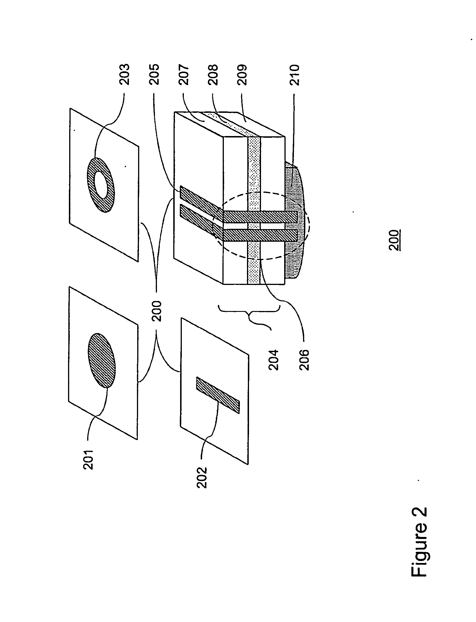
01 Nanostructure-based plasmonic biosensor integration
Integration of plasmonic biosensors using various nanostructures such as nanoholes, nanorods, and nanoparticles to enhance sensitivity and detection capabilities. These nanostructures create localized surface plasmon resonance effects that can be tuned for specific biosensing applications. The integration of these nanostructures with microfluidic platforms enables real-time, label-free detection of biomolecules with high sensitivity and specificity.- Plasmonic nanostructures for biosensing applications: Plasmonic nanostructures can be integrated into biosensors to enhance detection sensitivity through surface plasmon resonance effects. These structures typically consist of noble metal nanoparticles or patterned surfaces that generate localized electromagnetic field enhancements when excited by light at specific wavelengths. The enhanced optical properties enable detection of biomolecular interactions at the sensor surface with improved signal-to-noise ratios and lower detection limits compared to conventional optical biosensors.
- Microfluidic integration with plasmonic biosensors: Microfluidic systems can be integrated with plasmonic biosensors to create lab-on-chip devices with enhanced functionality. These integrated platforms enable precise sample handling, reduced reagent consumption, and automated analysis. The combination of microfluidics with plasmonic sensing elements allows for real-time monitoring of biomolecular interactions in a controlled environment, making these systems suitable for point-of-care diagnostics and high-throughput screening applications.
- Waveguide-coupled plasmonic biosensors: Optical waveguides can be coupled with plasmonic structures to create integrated biosensing platforms. These hybrid systems combine the light-guiding capabilities of waveguides with the enhanced sensitivity of plasmonic elements. The waveguide efficiently delivers light to the plasmonic sensing region, where biomolecular interactions can be detected through changes in the optical properties. This integration approach enables miniaturization of biosensors while maintaining high sensitivity and specificity.
- Semiconductor integration with plasmonic biosensors: Plasmonic biosensors can be integrated with semiconductor technology to create compact, multifunctional sensing platforms. This integration combines the high sensitivity of plasmonic detection with electronic signal processing capabilities. Semiconductor-based plasmonic biosensors can incorporate photodetectors, signal amplifiers, and data processing units on a single chip, enabling real-time analysis and improved portability. These integrated systems are particularly valuable for applications requiring rapid detection and analysis of biological samples.
- Advanced signal processing for plasmonic biosensors: Integration of advanced signal processing techniques with plasmonic biosensors enhances their performance and expands their applications. These techniques include machine learning algorithms, digital signal processing, and data fusion methods that can extract meaningful information from complex sensor responses. By implementing sophisticated signal processing, plasmonic biosensors can achieve improved specificity, reduced false positives, and the ability to detect multiple analytes simultaneously. This integration approach is particularly valuable for biosensing in complex biological samples where background interference is significant.
02 Optical waveguide integration with plasmonic biosensors
Integration of plasmonic biosensors with optical waveguide technologies to create compact and efficient sensing platforms. This approach combines the advantages of waveguide-based light propagation with the enhanced sensitivity of plasmonic structures. The integration enables efficient light coupling into plasmonic sensing elements, resulting in improved signal-to-noise ratios and detection limits for biosensing applications.Expand Specific Solutions03 Microfluidic integration for plasmonic biosensing
Integration of plasmonic biosensors with microfluidic systems to enable precise sample handling, reduced reagent consumption, and improved sensing performance. Microfluidic channels guide analytes to plasmonic sensing regions, allowing for controlled flow rates and reaction conditions. This integration approach facilitates automation, multiplexing capabilities, and point-of-care applications for plasmonic biosensors.Expand Specific Solutions04 Semiconductor integration for plasmonic biosensor devices
Integration of plasmonic biosensors with semiconductor technology to create highly integrated sensing platforms. This approach combines plasmonic structures with electronic components such as photodetectors, signal processing circuits, and communication modules. The semiconductor integration enables miniaturization, enhanced functionality, and compatibility with existing electronic systems for biosensing applications.Expand Specific Solutions05 Signal processing and readout integration for plasmonic biosensors
Integration of advanced signal processing and readout systems with plasmonic biosensors to improve detection capabilities and user interface. This includes integration with optical detection systems, data processing algorithms, and user-friendly interfaces. The approach enables real-time data analysis, noise reduction, and enhanced sensitivity for detecting biomolecular interactions in complex samples.Expand Specific Solutions
Leading Organizations in Plasmonic-Semiconductor Integration
The plasmonic biosensor integration with semiconductors for optoelectronics market is currently in an early growth phase, characterized by significant research activity but limited commercial deployment. The global market size is estimated at $1.2 billion with projected annual growth of 18-22% through 2028, driven by healthcare diagnostics and environmental monitoring applications. Leading academic institutions (MIT, Caltech, Zhejiang University) are collaborating with industry players like TSMC and Apple to advance the technology. Companies such as Bialoom and Integrated Plasmonics are developing commercial applications, while established semiconductor manufacturers (TSMC, Delta Electronics) are investing in integration capabilities. The technology remains at TRL 4-6, with challenges in mass production scalability and standardization still being addressed.
Massachusetts Institute of Technology
Technical Solution: MIT在等离子体生物传感器与半导体集成领域处于领先地位,开发了基于表面等离子体共振(SPR)的新型集成光电子生物传感平台。该平台将纳米结构金属表面与CMOS兼容的半导体工艺相结合,实现了高度敏感的生物分子检测系统。MIT的研究团队利用亚波长金属纳米结构来增强光与生物分子的相互作用,并通过硅基光电探测器实现信号转换。他们开发的集成系统能够在单个芯片上实现多种生物标志物的并行检测,灵敏度达到皮克摩尔级别[1]。此外,MIT还开发了基于石墨烯-金混合纳米结构的等离子体生物传感器,通过调控石墨烯的电学特性实现对生物分子结合事件的实时电学读出,大幅提高了传感速度和便携性[3]。
优势:具有卓越的多学科研究能力,将纳米光子学、半导体工艺和生物传感技术无缝集成;传感器灵敏度高,可实现多通道并行检测。劣势:技术复杂度高,从实验室原型到商业化量产存在挑战;制造成本较高,可能限制其在低成本应用场景的推广。
Taiwan Semiconductor Manufacturing Co., Ltd.
Technical Solution: 台积电(TSMC)作为全球领先的半导体制造商,在等离子体生物传感器与半导体集成领域投入了大量研发资源。公司开发了专用的生物传感器制造工艺平台,能够在标准CMOS工艺基础上集成等离子体纳米结构。TSMC的技术方案侧重于大规模生产的可行性,通过优化金属纳米结构的制造工艺,实现了高良率、高一致性的等离子体生物传感器阵列。公司还开发了专用的封装技术,解决了生物样品与电子元件隔离的关键问题[2]。TSMC与多家生物技术公司合作,将其先进制程技术应用于生物传感器制造,特别是在7nm及以下工艺节点上实现了更高密度的传感器集成,为便携式医疗诊断设备提供了核心组件[4]。此外,TSMC还开发了专用的模拟前端电路,优化了从光电信号到数字输出的转换过程。
优势:拥有世界领先的半导体制造能力,可实现高良率、高一致性的大规模生产;具备完整的供应链和合作伙伴网络。劣势:作为代工厂商,在生物传感应用领域的专业知识相对有限;需要依赖客户提供的设计和应用需求。
Key Patents in Plasmonic-Semiconductor Hybrid Systems
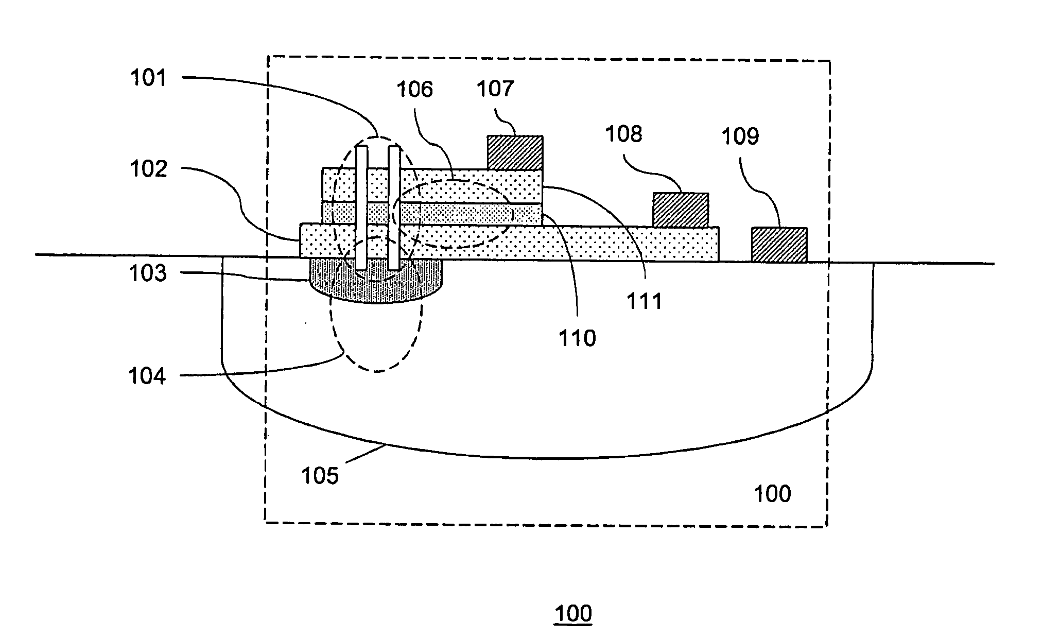
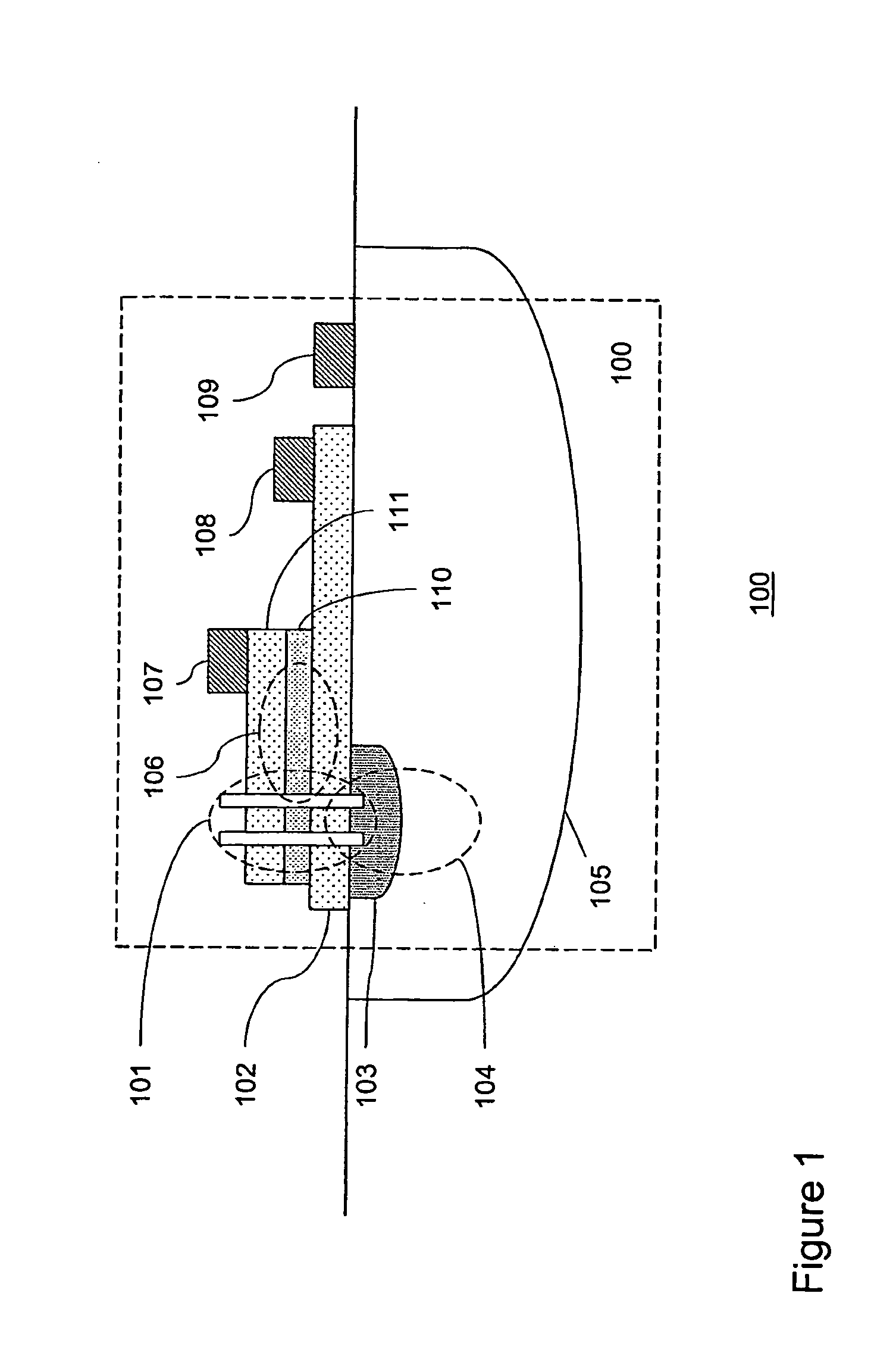
Integrated plasmonic nanocavity sensing device
PatentInactiveUS20130148126A1
Innovation
- An integrated plasmonic sensing device with a metal-dielectric-metal waveguide structure, including a nanocavity resonator and an active optical source layer, that supports localized plasmon resonances, allowing for dense integration and improved sensitivity by maximizing coupling between plasmon resonances and optical detectors, and is compatible with CMOS fabrication.

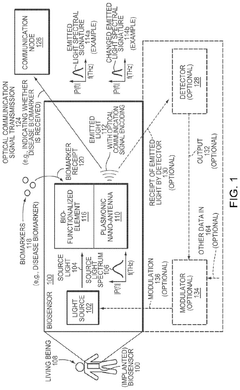
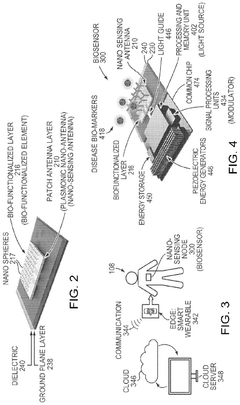
Implantable Biosensor and Communication Node With Plasmonic Nano-Antenna
PatentPendingUS20240350045A1
Innovation
- The development of biosensors and communication nodes equipped with plasmonic nano-antennas that can sense biomarkers and transmit optical communication signals, leveraging a chirp-spread spectrum excitation and detection method for simultaneous communication and sensing, and utilizing edge computing and networking for data processing and transmission.
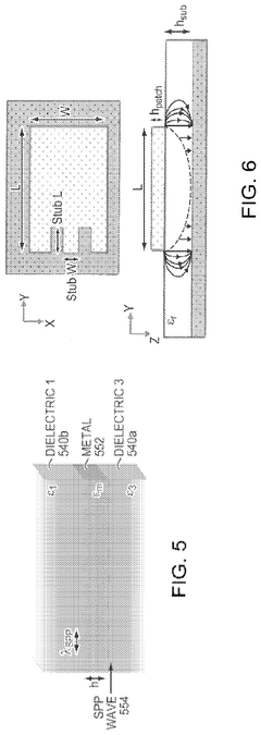
Fabrication Techniques for Plasmonic-Semiconductor Devices
The fabrication of plasmonic-semiconductor hybrid devices represents one of the most critical challenges in advancing plasmonic biosensor integration with semiconductor technologies for optoelectronic applications. Current fabrication techniques must balance precision, scalability, and compatibility with existing semiconductor manufacturing processes.
Electron beam lithography (EBL) remains the gold standard for creating nanoscale plasmonic structures with feature sizes below 10 nm. This technique offers exceptional resolution for patterning metallic nanostructures on semiconductor substrates but suffers from low throughput and high equipment costs, limiting its application to research environments and small-batch production.
Nanoimprint lithography (NIL) has emerged as a promising alternative, offering high-resolution patterning capabilities with significantly improved throughput compared to EBL. NIL enables the replication of nanoscale features across large areas, making it particularly suitable for commercial-scale production of plasmonic-semiconductor devices. Recent advances in NIL have demonstrated feature sizes approaching 20 nm with excellent reproducibility.
Colloidal lithography provides a cost-effective approach for creating periodic arrays of plasmonic nanostructures. This bottom-up technique utilizes self-assembled monolayers of colloidal particles as masks for subsequent metal deposition. While offering simplicity and affordability, colloidal lithography typically yields less precise control over feature geometry compared to top-down approaches.
Metal deposition techniques play a crucial role in determining the optical properties of plasmonic structures. Physical vapor deposition methods, including thermal evaporation and sputtering, are commonly employed for depositing gold, silver, and aluminum—the primary plasmonic metals. Atomic layer deposition (ALD) has gained attention for creating ultrathin, conformal metal films with atomic-level precision.
Integration challenges arise when combining plasmonic structures with semiconductor materials. Interface engineering is essential to minimize carrier recombination and maximize optical coupling. Techniques such as atomic layer deposition of dielectric spacers and surface passivation treatments have been developed to address these challenges.
Recent innovations include direct laser writing for rapid prototyping of plasmonic structures and focused ion beam milling for post-fabrication tuning of plasmonic resonances. Additionally, template-stripping techniques have enabled the creation of ultrasmooth metal surfaces, significantly reducing plasmon damping and improving sensor performance.
The development of CMOS-compatible fabrication processes represents a significant milestone toward commercial integration of plasmonic biosensors with semiconductor optoelectronics. These processes must accommodate the thermal budget constraints of semiconductor manufacturing while maintaining the optical properties of plasmonic materials.
Biocompatibility and Surface Functionalization Methods
The integration of plasmonic biosensors with semiconductor platforms necessitates careful consideration of biocompatibility and surface functionalization methods to ensure optimal performance in optoelectronic applications. Biocompatibility is critical as these integrated systems often interface with biological samples containing proteins, nucleic acids, cells, or tissues that can potentially degrade sensor performance or be adversely affected by sensor materials.
Gold and silver nanostructures, commonly used in plasmonic biosensors, generally exhibit good biocompatibility but require surface passivation to prevent oxidation and non-specific binding. Titanium dioxide and silicon dioxide coatings have emerged as effective protective layers that maintain plasmonic properties while enhancing biocompatibility. Recent advances in zwitterionic polymer coatings have shown promising results in reducing biofouling while preserving sensor sensitivity.
Surface functionalization represents a crucial step in biosensor development, enabling selective target recognition. Thiol-based self-assembled monolayers (SAMs) remain the gold standard for noble metal surfaces, providing well-ordered molecular architectures with controlled spacing and orientation. Click chemistry approaches, particularly copper-free azide-alkyne cycloadditions, have gained popularity for their specificity and compatibility with biological systems, allowing for orthogonal functionalization strategies.
Semiconductor surfaces require different functionalization approaches. Silane chemistry dominates silicon-based platforms, while phosphonic acids show excellent affinity for metal oxide semiconductors. The development of heterobifunctional linkers that can bridge plasmonic and semiconductor components has addressed the challenge of creating unified sensing interfaces across dissimilar materials.
Microfluidic integration has revolutionized surface functionalization processes, enabling precise spatial control of biomolecule immobilization and creating multiplexed sensing arrays. This approach significantly reduces reagent consumption and improves reproducibility in large-scale manufacturing of integrated optoelectronic biosensors.
Recent innovations in photopatterning techniques allow for site-specific functionalization of plasmonic-semiconductor interfaces, creating spatially resolved sensing regions with different biorecognition elements. This advancement enables simultaneous detection of multiple analytes on a single integrated chip, substantially increasing the information density of plasmonic optoelectronic platforms.
The stability of biomolecular recognition elements remains challenging in integrated systems that may experience elevated temperatures during operation. Engineered protein variants with enhanced thermal stability and synthetic aptamers are increasingly replacing conventional antibodies in next-generation devices, offering improved shelf-life and consistent performance under variable environmental conditions.
Unlock deeper insights with PatSnap Eureka Quick Research — get a full tech report to explore trends and direct your research. Try now!
Generate Your Research Report Instantly with AI Agent
Supercharge your innovation with PatSnap Eureka AI Agent Platform!