Standards Governing the Use of Plasmonic Biosensors in Electronics
SEP 29, 20259 MIN READ
Generate Your Research Report Instantly with AI Agent
Patsnap Eureka helps you evaluate technical feasibility & market potential.
Plasmonic Biosensor Standards Evolution and Objectives
Plasmonic biosensor technology has evolved significantly over the past three decades, transitioning from academic research curiosities to commercially viable electronic sensing platforms. The field emerged in the early 1990s with the discovery that surface plasmon resonance (SPR) could be harnessed for label-free biomolecular detection. Initial standards focused primarily on optical configurations and basic sensing parameters, with limited consideration for electronic integration.
By the early 2000s, the miniaturization trend in electronics catalyzed efforts to standardize plasmonic biosensor components for portable applications. This period saw the establishment of preliminary guidelines by organizations such as ASTM International and IEEE, addressing fundamental aspects like signal-to-noise ratios, detection limits, and reproducibility metrics specifically for electronic implementations of plasmonic sensing.
The 2010s marked a significant evolution in standardization approaches, with the International Organization for Standardization (ISO) developing the ISO/TC 229 framework for nanotechnologies, which included specific provisions for plasmonic nanomaterials in biosensing applications. Concurrently, the International Electrotechnical Commission (IEC) introduced standards addressing the electronic interfaces and signal processing requirements for integrated plasmonic biosensors.
Current standardization efforts are increasingly focused on interoperability, reliability, and performance benchmarking across different plasmonic biosensor platforms. The SEMI organization has recently introduced standards specifically addressing the integration of plasmonic elements with semiconductor manufacturing processes, facilitating mass production of electronically-controlled biosensing devices.
The primary objectives of contemporary plasmonic biosensor standards include establishing universal performance metrics, ensuring measurement reproducibility across different laboratories and manufacturing facilities, and facilitating regulatory approval processes for commercial applications. These standards aim to bridge the gap between fundamental plasmonic physics and practical electronic implementation.
Looking forward, emerging standardization goals include addressing the integration of plasmonic biosensors with advanced electronic architectures such as flexible electronics, Internet of Things (IoT) platforms, and artificial intelligence systems. Standards development organizations are increasingly recognizing the need for guidelines that accommodate novel plasmonic materials, including graphene-based plasmonics and quantum plasmonic effects, which promise unprecedented sensitivity and selectivity in next-generation electronic biosensors.
The convergence of electronics and plasmonic biosensing technologies necessitates evolving standards that can address multidisciplinary challenges spanning nanofabrication, optoelectronics, biochemistry, and data science. Future standardization objectives will likely focus on establishing protocols for validating multiplexed sensing capabilities and defining performance requirements for real-time, continuous monitoring applications in healthcare and environmental sensing.
Market Analysis for Plasmonic Biosensors in Electronics
The global market for plasmonic biosensors in electronics is experiencing robust growth, driven by increasing demand for rapid, sensitive, and portable diagnostic solutions across multiple industries. Current market valuations place the plasmonic biosensor segment at approximately 1.2 billion USD in 2023, with projections indicating a compound annual growth rate (CAGR) of 8.7% through 2030, potentially reaching 2.1 billion USD by the end of the forecast period.
Healthcare and biomedical applications currently dominate the market landscape, accounting for nearly 45% of total market share. This dominance stems from the critical need for early disease detection, point-of-care diagnostics, and pharmaceutical research applications. The COVID-19 pandemic significantly accelerated market adoption, as plasmonic biosensors demonstrated exceptional utility in rapid viral detection scenarios.
Environmental monitoring represents the second-largest application segment, comprising approximately 20% of the market. Growing concerns regarding water quality, air pollution, and food safety have spurred demand for highly sensitive detection methods capable of identifying contaminants at extremely low concentrations. Plasmonic biosensors' ability to detect specific molecular targets with minimal sample preparation has positioned them as ideal solutions for environmental monitoring challenges.
Regional analysis reveals North America as the current market leader, holding approximately 38% of global market share, followed by Europe (29%) and Asia-Pacific (24%). However, the Asia-Pacific region is expected to witness the fastest growth rate over the next five years, driven by increasing healthcare expenditure, expanding research infrastructure, and growing environmental concerns in countries like China, Japan, and India.
Key market restraints include high initial development costs, technical complexity in standardization, and competition from alternative sensing technologies. The average cost of implementing plasmonic biosensor systems remains significantly higher than conventional detection methods, limiting widespread adoption in cost-sensitive markets and developing economies.
Consumer electronics applications represent an emerging high-growth segment, with wearable health monitoring devices incorporating plasmonic sensing technology showing particular promise. Market analysts predict this segment could grow at twice the overall market rate, potentially reaching 15% CAGR through 2030 as miniaturization advances and production costs decrease.
Market consolidation is becoming increasingly evident, with major players pursuing strategic acquisitions to expand technology portfolios and geographic reach. Simultaneously, numerous startups are entering the space with novel applications and implementation approaches, creating a dynamic competitive landscape characterized by both innovation and integration.
Global Technological Landscape and Barriers
The global landscape for plasmonic biosensor technology in electronics reveals significant disparities in development and implementation across different regions. North America, particularly the United States, maintains leadership in research output and patent filings, with major institutions like MIT, Stanford University, and national laboratories driving innovation. The European Union follows closely, with countries like Germany, France, and the United Kingdom contributing substantial research through institutions such as Max Planck Institutes and Imperial College London.
In Asia, Japan and South Korea have established strong positions in plasmonic biosensor manufacturing capabilities, while China is rapidly closing the gap through aggressive investment in both fundamental research and commercial applications. Other regions, including Latin America, Africa, and parts of Southeast Asia, remain largely consumers rather than developers of this technology.
Despite global progress, several critical barriers impede widespread adoption of plasmonic biosensors in electronics. Technical challenges include achieving consistent reproducibility in nanofabrication processes at commercial scales. The precise control required for plasmonic structures often results in high manufacturing costs and yield inconsistencies, limiting mass production capabilities.
Standardization represents another significant hurdle. The absence of universally accepted protocols for performance evaluation, calibration, and validation creates market fragmentation and hampers interoperability between different systems. This lack of standardization also complicates regulatory approval processes across different jurisdictions.
Regulatory frameworks vary substantially between regions, creating compliance challenges for global manufacturers. While the FDA in the United States and similar bodies in Europe have established pathways for certain biosensor applications, many countries lack specific regulations addressing the unique characteristics of plasmonic technologies, particularly when integrated into electronic systems.
Knowledge transfer barriers also exist between academic research and industrial implementation. The highly specialized expertise required for plasmonic biosensor development creates workforce limitations, with insufficient training programs to meet industry demand for qualified specialists.
Infrastructure limitations present additional challenges, particularly in emerging markets. The sophisticated equipment required for both manufacturing and quality control of plasmonic components necessitates significant capital investment, creating entry barriers for smaller companies and developing economies.
Addressing these global disparities and overcoming technical, regulatory, and infrastructure barriers will be essential for realizing the full potential of plasmonic biosensors in next-generation electronic applications.
Current Standardization Frameworks and Implementations
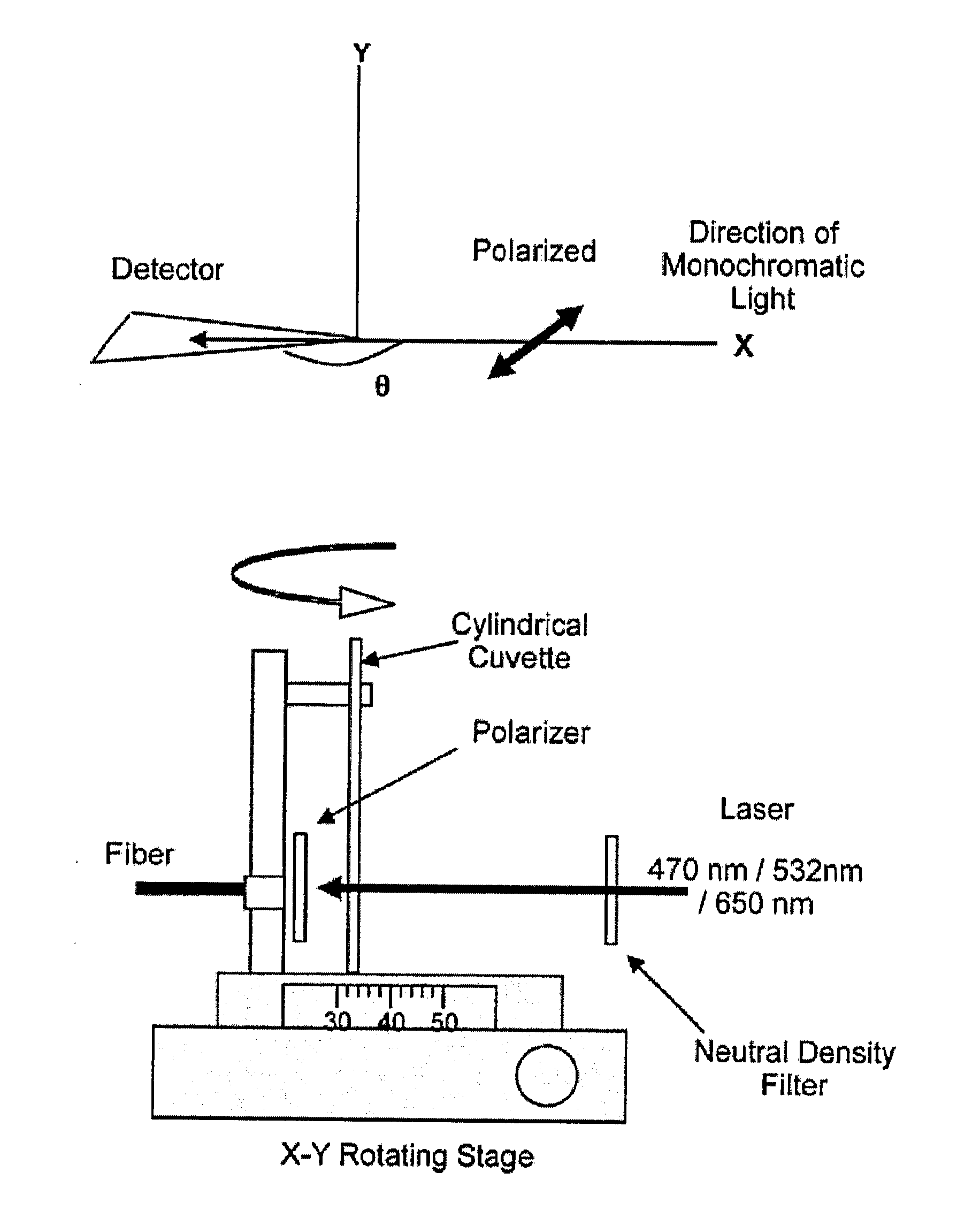
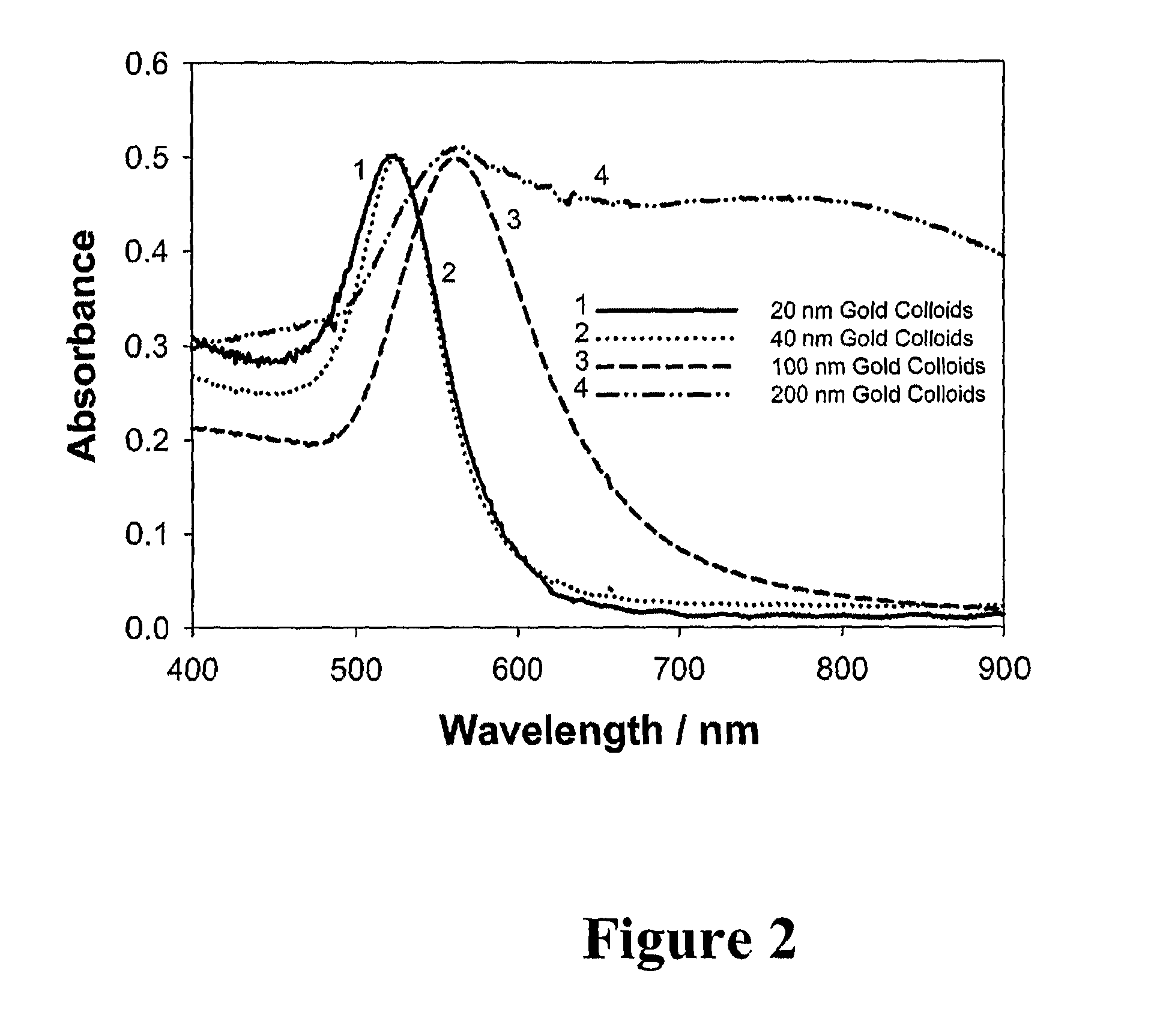
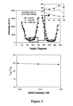
01 Surface plasmon resonance (SPR) biosensor technology
Surface plasmon resonance biosensors utilize the optical phenomenon of SPR to detect biomolecular interactions at metal-dielectric interfaces. These biosensors offer label-free, real-time detection with high sensitivity for various analytes. The technology employs metallic nanostructures (typically gold or silver) that generate surface plasmons when illuminated with light at specific wavelengths, creating evanescent fields highly sensitive to refractive index changes caused by molecular binding events at the sensor surface.- Surface plasmon resonance (SPR) biosensor design: Surface plasmon resonance biosensors utilize the interaction between electromagnetic waves and conductive surfaces to detect biomolecular interactions. These designs typically incorporate metallic nanostructures that enhance sensitivity through localized surface plasmon resonance effects. The sensors can detect minute changes in refractive index when target analytes bind to functionalized surfaces, making them highly effective for label-free detection of biomolecules with applications in medical diagnostics and environmental monitoring.
- Nanostructured plasmonic materials for enhanced sensitivity: Nanostructured materials such as gold and silver nanoparticles, nanorods, and nanoholes are incorporated into plasmonic biosensors to enhance detection sensitivity. These nanostructures create strong electromagnetic field enhancements at their surfaces, known as hot spots, which significantly improve the detection limits of the biosensors. Various fabrication techniques including lithography, self-assembly, and template-assisted growth are used to create these nanostructured surfaces with precisely controlled geometries for optimal plasmonic performance.
- Integration of plasmonic biosensors with microfluidic systems: Combining plasmonic biosensors with microfluidic platforms creates integrated lab-on-chip devices that enable precise sample handling, reduced reagent consumption, and multiplexed detection capabilities. These integrated systems facilitate real-time monitoring of biomolecular interactions with improved throughput and automation. The microfluidic channels direct analytes to specific sensing regions, enhancing the efficiency of the detection process while minimizing sample volume requirements, making them suitable for point-of-care diagnostic applications.
- Signal processing and data analysis methods for plasmonic biosensors: Advanced signal processing algorithms and data analysis methods are developed to extract meaningful information from plasmonic biosensor measurements. These techniques include noise reduction algorithms, pattern recognition, machine learning approaches, and statistical analysis methods that improve the accuracy and reliability of detection. Real-time data processing enables rapid analysis of binding kinetics and quantification of target analytes, enhancing the overall performance and practical utility of plasmonic biosensor systems.
- Waveguide-coupled plasmonic biosensor configurations: Optical waveguide structures are integrated with plasmonic elements to create highly sensitive biosensing platforms. These configurations guide light to interact with plasmonic nanostructures at specific locations, enabling efficient coupling between guided modes and surface plasmons. The waveguide-coupled designs offer advantages including improved light management, enhanced sensor miniaturization, and compatibility with existing photonic integrated circuits. These systems can be fabricated using standard semiconductor processing techniques, facilitating their integration into portable sensing devices.
02 Nanostructured plasmonic materials for enhanced sensitivity
Nanostructured plasmonic materials, including nanoparticles, nanorods, and nanopatterned surfaces, are engineered to enhance biosensor sensitivity through localized surface plasmon resonance (LSPR). These nanostructures create intense electromagnetic field hotspots that amplify detection signals, enabling the sensing of smaller analytes or lower concentrations. Various fabrication techniques are employed to create these nanostructures with precise dimensions and arrangements to optimize their plasmonic properties for specific biosensing applications.Expand Specific Solutions03 Integration of plasmonic biosensors with microfluidics
Integrating plasmonic biosensors with microfluidic systems creates lab-on-a-chip devices that enable precise sample handling, reduced reagent consumption, and multiplexed detection capabilities. These integrated systems facilitate automated sample preparation, controlled flow conditions, and real-time monitoring of biomolecular interactions. The combination enhances throughput, reproducibility, and practical applicability of plasmonic biosensors for point-of-care diagnostics and environmental monitoring applications.Expand Specific Solutions04 Waveguide-coupled plasmonic biosensors
Waveguide-coupled plasmonic biosensors combine optical waveguide technology with plasmonic sensing elements to achieve highly sensitive and miniaturized detection platforms. These hybrid systems guide light to specific sensing regions where plasmonic structures interact with analytes, enabling efficient light-matter interactions and signal transduction. The waveguide architecture allows for compact device designs, multiplexed sensing capabilities, and integration with existing optical components, making them suitable for portable diagnostic applications.Expand Specific Solutions05 Signal processing and data analysis for plasmonic biosensors
Advanced signal processing and data analysis techniques are crucial for extracting meaningful information from plasmonic biosensor measurements. These methods include noise reduction algorithms, multivariate analysis, machine learning approaches, and real-time data processing to improve detection limits and specificity. Signal enhancement strategies, calibration techniques, and reference channel designs are implemented to compensate for environmental interferences and non-specific binding, ensuring reliable and quantitative biosensing results in complex sample matrices.Expand Specific Solutions
Industry Leaders and Competitive Ecosystem
The plasmonic biosensor market in electronics is currently in a growth phase, characterized by increasing research activity and emerging commercial applications. The market size is expanding due to rising demand for rapid, sensitive detection systems in healthcare, environmental monitoring, and security sectors. Technologically, the field shows varying maturity levels across players. Leading research institutions like University of California and Yale University are pioneering fundamental innovations, while companies such as Applied Materials, Intel, and Hitachi are developing practical implementations. Smaller specialized firms like Onechip Bioelectronics and Hoth Therapeutics are focusing on niche applications. Standards development remains fragmented, with collaborative efforts between academic institutions, industry leaders, and regulatory bodies like the Government of the United States working to establish unified protocols for reliability, sensitivity, and interoperability.
The Regents of the University of California
Technical Solution: The University of California has developed advanced plasmonic biosensor platforms that integrate nanophotonic structures with electronic readout systems. Their approach focuses on surface plasmon resonance (SPR) sensors with enhanced sensitivity through nanostructured metal films. They've pioneered the development of CMOS-compatible plasmonic biosensors that can be directly integrated with electronic circuits, enabling point-of-care diagnostic applications. Their technology utilizes gold nanoparticles and nanorods with precisely controlled geometries to achieve localized surface plasmon resonance (LSPR) with detection limits in the femtomolar range. UC researchers have also established standardized fabrication protocols that ensure reproducibility across different manufacturing facilities, addressing one of the key challenges in commercializing plasmonic biosensors. Their work includes comprehensive characterization methods that have been adopted by other institutions as de facto standards for performance validation[1][3].
Strengths: Exceptional sensitivity reaching femtomolar detection limits; seamless integration with existing CMOS technology; established standardized fabrication protocols. Weaknesses: Higher production costs compared to conventional biosensors; requires specialized equipment for nanofabrication; gold-based platforms may face long-term stability issues in certain environments.
Applied Materials, Inc.
Technical Solution: Applied Materials has developed specialized deposition and etching equipment specifically optimized for plasmonic biosensor fabrication. Their technology focuses on creating uniform, high-quality metal films with precisely controlled thickness and optical properties critical for plasmonic applications. They've established manufacturing standards for gold, silver, and aluminum thin films with thickness variations below 1nm across 300mm wafers, enabling consistent biosensor performance. Applied Materials' equipment incorporates in-situ monitoring tools that verify plasmonic properties during fabrication, ensuring that devices meet predefined performance specifications. Their process technology enables the creation of nanostructured surfaces with feature sizes down to 10nm, which is essential for high-sensitivity LSPR biosensors. The company has also developed cleaning and passivation protocols that preserve the optical properties of plasmonic materials while making them compatible with biological samples and electronic integration requirements[4][7].
Strengths: Unmatched precision in thin film deposition; comprehensive quality control systems; established protocols for maintaining plasmonic material properties. Weaknesses: Equipment requires significant capital investment; specialized processes may limit flexibility; solutions primarily focused on manufacturing rather than complete biosensor systems.
Key Patents and Technical Literature Analysis
Bioassays using plasmonic scattering from noble metal nanostructures
PatentInactiveUS20100062545A1
Innovation
- The use of surface plasmons from metallic nanoparticles to measure scattering effects at different angles and wavelengths, allowing for the detection of analyte concentration through changes in intensity and polarization, which is more stable and sensitive than traditional methods by utilizing the superior scattering properties of noble metal nanostructures.
Clusters of microresonators for cavity mode optical sensing
PatentWO2009084721A1
Innovation
- The development of clusters of microresonators that are positioned in close vicinity to each other, allowing for the generation of characteristic spectral fingerprints through wavelength shifts of optical cavity modes for molecular detection, enabling improved sensitivity and multiplexing capabilities.
Regulatory Compliance and Certification Requirements
The regulatory landscape for plasmonic biosensors in electronics is complex and multifaceted, requiring adherence to standards across multiple domains. Medical Device Regulations such as FDA's 510(k) clearance in the US and the EU's Medical Device Regulation (MDR) apply when these biosensors are integrated into diagnostic equipment. These frameworks mandate rigorous clinical validation, risk assessment, and post-market surveillance protocols specific to nanomaterial-based sensing technologies.
Environmental compliance presents another critical regulatory dimension, with the Restriction of Hazardous Substances (RoHS) and Registration, Evaluation, Authorization and Restriction of Chemicals (REACH) regulations imposing strict limitations on potentially harmful materials used in plasmonic structures. Manufacturers must document the precise composition of noble metals and nanoparticles, while demonstrating appropriate end-of-life management strategies for these specialized components.
Electromagnetic compatibility (EMC) certification requirements are particularly relevant for plasmonic biosensors, which often operate alongside sensitive electronic systems. Standards such as IEC 61326 specifically address electrical equipment for measurement, control, and laboratory use, requiring manufacturers to demonstrate that plasmonic components neither cause nor are susceptible to electromagnetic interference. This necessitates specialized testing protocols that account for the unique optical-electronic interfaces present in these systems.
Nanomaterial-specific regulations are emerging as critical compliance factors. The ISO/TC 229 framework provides standardized approaches for characterization and toxicological assessment of engineered nanomaterials, while OECD guidelines establish testing protocols for nanomaterial safety. These standards are increasingly referenced in regulatory submissions for plasmonic biosensors, which typically incorporate gold, silver, or other metallic nanostructures.
Quality management certification, particularly ISO 13485 for medical devices and ISO 9001 for general electronics manufacturing, establishes the procedural framework for consistent production of plasmonic biosensors. These standards mandate documented processes for design control, supplier management, and production consistency—critical factors for technologies where nanoscale precision directly impacts sensing performance.
International harmonization efforts are gradually addressing regulatory fragmentation through initiatives like the International Medical Device Regulators Forum (IMDRF) and the Global Harmonization Task Force (GHTF). These collaborations are developing consensus documents specifically addressing novel sensing technologies, though significant regional variations in implementation persist, creating compliance challenges for global manufacturers of plasmonic biosensor systems.
Cross-Industry Applications and Integration Challenges
Plasmonic biosensors are experiencing unprecedented cross-industry adoption, extending far beyond their traditional applications in healthcare diagnostics. The integration of these advanced sensing technologies into electronics has created new opportunities in environmental monitoring, food safety, security systems, and consumer electronics. In environmental applications, plasmonic biosensors enable real-time detection of pollutants and toxins at previously undetectable concentrations, revolutionizing how industries monitor their environmental impact and comply with increasingly stringent regulations.
The food and beverage industry has embraced plasmonic biosensor technology for rapid pathogen detection and quality control throughout the supply chain. These sensors provide immediate results without the need for time-consuming laboratory analysis, significantly reducing the risk of contaminated products reaching consumers and enabling more efficient production processes. Similarly, in security and defense applications, plasmonic biosensors offer capabilities for detecting biological threats and explosives with heightened sensitivity and specificity.
Despite these promising applications, significant integration challenges persist across industries. The primary technical hurdle involves miniaturization and compatibility with existing electronic systems. While plasmonic biosensors excel in laboratory settings, adapting them to compact, field-deployable devices requires overcoming complex engineering challenges related to signal processing, power requirements, and form factor constraints. This is particularly evident in consumer electronics, where space limitations and cost considerations create additional barriers to implementation.
Standardization represents another critical challenge. The lack of unified protocols for calibration, validation, and performance metrics has created a fragmented landscape where cross-platform comparability remains difficult. This absence of standardization impedes widespread adoption and creates uncertainty for manufacturers looking to incorporate plasmonic biosensing capabilities into their electronic products. Industry consortia and standards organizations have only recently begun addressing these issues, with preliminary frameworks emerging for specific applications rather than comprehensive cross-industry standards.
Data integration presents a third significant challenge. Plasmonic biosensors generate complex datasets that must be effectively processed, analyzed, and integrated with existing information systems. This requires sophisticated algorithms and data management protocols that can operate within the constraints of various electronic platforms. The development of standardized data formats and interpretation methodologies remains an active area of research, with potential solutions emerging from collaborative efforts between sensor manufacturers, electronics companies, and data science specialists.
Unlock deeper insights with Patsnap Eureka Quick Research — get a full tech report to explore trends and direct your research. Try now!
Generate Your Research Report Instantly with AI Agent
Supercharge your innovation with Patsnap Eureka AI Agent Platform!