Comparative Analysis of Plasmonic Biosensors in Semiconductor Applications
SEP 29, 202510 MIN READ
Generate Your Research Report Instantly with AI Agent
Patsnap Eureka helps you evaluate technical feasibility & market potential.
Plasmonic Biosensor Evolution and Objectives
Plasmonic biosensors have undergone significant evolution since their inception in the late 1980s, transforming from rudimentary surface plasmon resonance (SPR) devices to sophisticated integrated semiconductor platforms. The initial development phase focused primarily on basic SPR principles utilizing gold films, with limited sensitivity and application scope. These early sensors operated on the fundamental principle of detecting refractive index changes at metal-dielectric interfaces when biomolecular binding events occurred.
The mid-1990s marked a pivotal transition with the introduction of localized surface plasmon resonance (LSPR) techniques, which leveraged metallic nanostructures to enhance field confinement and sensitivity. This advancement expanded the application potential beyond laboratory settings, enabling more compact designs and reduced sample volume requirements. The integration with semiconductor manufacturing processes began to emerge during this period, though remained largely experimental.
By the early 2000s, plasmonic biosensors entered a phase of rapid technological advancement with the development of nanostructured plasmonic arrays and the incorporation of microfluidic systems. These innovations significantly improved detection limits and enabled multiplexed sensing capabilities. The convergence with semiconductor technology accelerated, particularly through the adoption of complementary metal-oxide-semiconductor (CMOS) compatible fabrication techniques.
The past decade has witnessed transformative progress in plasmonic biosensor technology, characterized by the seamless integration with semiconductor platforms. Advanced nanofabrication methods have enabled the creation of complex plasmonic architectures with unprecedented sensitivity and specificity. Notable developments include the emergence of hybrid plasmonic-photonic structures, quantum plasmonic sensors, and active plasmonic devices with tunable properties.
Current research objectives in plasmonic biosensor development for semiconductor applications focus on several key areas. First, enhancing detection sensitivity to achieve single-molecule detection capabilities while maintaining high throughput. Second, improving selectivity through surface functionalization strategies and novel recognition elements. Third, developing fully integrated lab-on-chip platforms that combine sensing, sample preparation, and data processing functionalities.
Additional objectives include reducing manufacturing costs through scalable fabrication techniques compatible with existing semiconductor processes, minimizing power consumption for portable and implantable applications, and improving long-term stability under various environmental conditions. The ultimate goal is to develop next-generation plasmonic biosensors that can be seamlessly integrated into semiconductor devices for real-time, in-situ monitoring in diverse fields including healthcare diagnostics, environmental monitoring, food safety, and pharmaceutical development.
Semiconductor Industry Demand for Biosensing Technologies
The semiconductor industry is experiencing a significant shift towards integrating biosensing technologies into its manufacturing processes and end products. This growing demand is driven by several converging factors, including the need for more sophisticated quality control measures, environmental monitoring requirements, and the expansion into healthcare applications. Plasmonic biosensors, with their unique capabilities for label-free, real-time detection of biological and chemical analytes, are particularly well-positioned to address these emerging needs.
Manufacturing process control represents one of the most immediate applications for biosensing technologies in semiconductor fabrication. As chip architectures become increasingly complex and feature sizes continue to shrink below 5nm, traditional optical inspection methods are reaching their physical limits. Plasmonic biosensors offer unprecedented sensitivity for detecting molecular contaminants that can compromise yield rates. Industry data indicates that even sub-parts-per-billion contamination levels can significantly impact production outcomes in advanced node processes.
Environmental monitoring within semiconductor fabrication facilities constitutes another critical application area. The ultra-clean environments required for modern semiconductor manufacturing necessitate continuous monitoring of airborne molecular contaminants and particulates. Plasmonic biosensors enable real-time detection of specific biological and chemical agents that traditional particulate counters cannot identify, helping maintain the stringent cleanliness standards required for high-yield production.
The integration of sensing capabilities directly into semiconductor devices represents a major growth vector for the industry. As the Internet of Things (IoT) ecosystem expands, demand for chips with integrated sensing capabilities is accelerating across multiple sectors including consumer electronics, automotive, and industrial applications. Market analyses project that semiconductor-based sensing components will grow at a compound annual rate exceeding the broader semiconductor market over the next five years.
Healthcare applications present perhaps the most transformative opportunity for semiconductor-based biosensing technologies. The convergence of semiconductor manufacturing expertise with biosensing capabilities is enabling a new generation of point-of-care diagnostic devices, continuous health monitoring systems, and implantable medical devices. These applications leverage the miniaturization capabilities of semiconductor manufacturing to create highly sensitive, portable, and cost-effective biosensing platforms.
Sustainability considerations are also driving demand for advanced biosensing capabilities in semiconductor manufacturing. As regulatory requirements for environmental monitoring become more stringent globally, semiconductor manufacturers must implement more sophisticated systems for detecting and quantifying potential biological and chemical emissions. Plasmonic biosensors offer the sensitivity and specificity needed to meet these evolving compliance requirements while maintaining operational efficiency.
Current Plasmonic Biosensor Limitations in Semiconductor Integration
Despite the promising potential of plasmonic biosensors in semiconductor applications, several significant limitations currently hinder their widespread integration and commercial adoption. The primary challenge lies in the inherent incompatibility between traditional plasmonic materials and standard semiconductor manufacturing processes. Gold and silver, the most commonly used plasmonic metals, are considered contaminants in CMOS fabrication environments, necessitating complex isolation strategies that increase manufacturing complexity and cost.
Miniaturization presents another substantial obstacle. While semiconductor technology continues to shrink following Moore's Law, plasmonic structures face fundamental physical limitations when scaled down below certain dimensions. At nanoscale sizes, plasmonic resonances can become unstable or exhibit significantly reduced sensitivity, compromising the core advantage of these biosensing platforms.
Thermal stability issues further complicate integration efforts. Plasmonic materials, particularly noble metals, often have different thermal expansion coefficients compared to semiconductor substrates. This mismatch creates stress during thermal cycling in manufacturing processes, potentially leading to delamination, cracking, or performance degradation over time.
Signal-to-noise ratio optimization remains problematic in integrated environments. The proximity of plasmonic sensors to semiconductor components introduces electronic noise that can mask the often subtle optical signals generated by biomolecular interactions. Current isolation techniques add complexity without fully resolving this fundamental challenge.
Reproducibility in mass manufacturing represents a significant barrier to commercialization. The performance of plasmonic biosensors is highly dependent on precise nanoscale geometries and surface properties. Maintaining consistent quality across thousands of devices on semiconductor wafers requires manufacturing precision beyond current industrial capabilities.
Biocompatibility concerns also emerge when integrating biological recognition elements with semiconductor platforms. The surface chemistry required for biomolecule immobilization must be compatible with both the plasmonic structures and the surrounding semiconductor materials, creating a complex interface engineering challenge.
Power consumption presents another limitation, particularly for portable or implantable applications. While passive plasmonic structures themselves require no power, the associated light sources, detectors, and signal processing components necessary for a complete sensing system can demand significant energy resources, limiting their utility in resource-constrained environments.
Contemporary Plasmonic Biosensor Integration Solutions
01 Plasmonic nanostructures for enhanced biosensing
Plasmonic biosensors utilize nanostructures such as gold or silver nanoparticles that exhibit localized surface plasmon resonance (LSPR) to enhance detection sensitivity. These nanostructures can be engineered with specific geometries and arrangements to amplify the biosensing signal. The interaction between biomolecules and the plasmonic nanostructures causes measurable shifts in the resonance wavelength, enabling highly sensitive detection of biological analytes.- Plasmonic nanostructures for enhanced biosensing: Plasmonic biosensors utilize nanostructures such as gold or silver nanoparticles that exhibit localized surface plasmon resonance (LSPR) to enhance detection sensitivity. These nanostructures create strong electromagnetic field enhancements when excited by light at specific wavelengths, allowing for label-free detection of biomolecules. The plasmonic properties can be tuned by controlling the size, shape, and composition of the nanostructures, enabling detection of various analytes at low concentrations.
- Integration of plasmonic biosensors with microfluidic systems: Combining plasmonic biosensors with microfluidic platforms creates integrated lab-on-chip devices for point-of-care diagnostics. These systems enable precise sample handling, reduced reagent consumption, and faster analysis times. Microfluidic channels direct analytes to plasmonic sensing regions, allowing for multiplexed detection of multiple biomarkers simultaneously. This integration enhances the practical applicability of plasmonic biosensors in clinical settings and field-deployable devices.
- Waveguide-coupled plasmonic biosensors: Waveguide-coupled plasmonic biosensors combine optical waveguides with plasmonic structures to improve light-matter interactions and sensing capabilities. These hybrid systems guide light to plasmonic sensing regions, enabling efficient excitation of surface plasmons and collection of optical signals. The integration of waveguides allows for miniaturization and on-chip integration of multiple sensing elements, making these biosensors suitable for compact, high-throughput diagnostic platforms.
- Signal processing and readout methods for plasmonic biosensors: Advanced signal processing techniques and readout methods enhance the performance of plasmonic biosensors by improving signal-to-noise ratios and detection limits. These include phase-sensitive detection, spectral analysis, and machine learning algorithms for data interpretation. Novel readout approaches such as smartphone-based detection systems make plasmonic biosensors more accessible for field applications and resource-limited settings, enabling real-time monitoring and rapid diagnostics.
- Surface functionalization strategies for selective biomolecule detection: Surface functionalization of plasmonic biosensors with specific recognition elements enables selective detection of target biomolecules. Various surface chemistry approaches are used to immobilize antibodies, aptamers, or other biorecognition molecules onto plasmonic surfaces while minimizing non-specific binding. These functionalization strategies improve the specificity and sensitivity of plasmonic biosensors for applications in medical diagnostics, environmental monitoring, and food safety testing.
02 Integrated optical waveguide plasmonic biosensors
These biosensors combine plasmonic elements with optical waveguide technology to create compact and sensitive detection platforms. The integration allows for efficient light coupling into the plasmonic structures and facilitates miniaturization of the sensing devices. Waveguide-based plasmonic biosensors enable real-time monitoring of biomolecular interactions with high sensitivity and are suitable for lab-on-a-chip applications.Expand Specific Solutions03 Surface-enhanced Raman spectroscopy (SERS) biosensors
SERS-based plasmonic biosensors utilize the enhancement of Raman signals by plasmonic nanostructures to detect biomolecules with high specificity. The plasmonic effect amplifies the Raman scattering from molecules near the metal surface by several orders of magnitude, enabling detection at extremely low concentrations. These biosensors can provide molecular fingerprint information and are particularly useful for detecting specific biomarkers in complex biological samples.Expand Specific Solutions04 Microfluidic plasmonic biosensor systems
Integration of plasmonic biosensors with microfluidic systems enables automated sample handling, reduced reagent consumption, and multiplexed detection capabilities. These systems incorporate channels, chambers, and valves to control fluid flow over the plasmonic sensing elements. Microfluidic plasmonic biosensors are particularly advantageous for point-of-care diagnostics and high-throughput screening applications where sample volume is limited.Expand Specific Solutions05 Novel materials and fabrication techniques for plasmonic biosensors
Advanced materials and fabrication methods are being developed to enhance the performance of plasmonic biosensors. These include novel plasmonic materials beyond traditional gold and silver, such as aluminum and conductive oxides, as well as innovative nanofabrication techniques like nanoimprint lithography and self-assembly. These approaches enable the creation of more stable, sensitive, and cost-effective plasmonic biosensing platforms with improved reproducibility and scalability.Expand Specific Solutions
Leading Companies and Research Institutions in Plasmonic Biosensing
The plasmonic biosensor market in semiconductor applications is currently in a growth phase, characterized by increasing adoption across healthcare, environmental monitoring, and biodefense sectors. The global market size is projected to expand significantly, driven by demand for rapid, sensitive detection technologies. Technologically, the field shows varying maturity levels among key players: established semiconductor giants like TSMC, Intel, and IBM lead with advanced manufacturing capabilities and integration expertise, while specialized companies such as X-Body and Hoth Therapeutics focus on novel biosensing applications. Academic institutions including MIT, Washington University, and Northeastern University contribute fundamental research advancements. The competitive landscape reflects a productive ecosystem where commercial development is accelerated through industry-academia collaborations, particularly in nanofabrication techniques and surface plasmon resonance optimization.
Taiwan Semiconductor Manufacturing Co., Ltd.
Technical Solution: TSMC has developed advanced plasmonic biosensor technology integrated with their semiconductor manufacturing processes. Their approach utilizes surface plasmon resonance (SPR) phenomena on metallic nanostructures fabricated using their industry-leading sub-7nm process nodes. TSMC's plasmonic biosensors incorporate gold and silver nanoparticles precisely deposited on semiconductor substrates to create highly sensitive detection platforms. The company has demonstrated detection limits in the femtomolar range for various biomolecules by optimizing the plasmonic coupling between nanostructures. Their technology employs CMOS-compatible processes to create plasmonic waveguides that can be directly integrated with signal processing circuitry, enabling complete lab-on-chip solutions. TSMC has also pioneered the use of aluminum as a cost-effective alternative to gold in certain plasmonic applications, maintaining sensitivity while reducing manufacturing costs.
Strengths: Industry-leading nanofabrication capabilities allow for precise control of plasmonic structures; seamless integration with existing semiconductor manufacturing infrastructure; high volume production capability. Weaknesses: Higher production costs compared to traditional biosensors; gold-based plasmonic structures face challenges in CMOS compatibility; limited flexibility for customization in high-volume manufacturing.
International Business Machines Corp.
Technical Solution: IBM has developed a novel plasmonic biosensor platform that leverages their expertise in semiconductor manufacturing and nanophotonics. Their approach utilizes silicon photonics integrated with plasmonic nanostructures to create highly sensitive biosensing devices. IBM's technology employs a hybrid architecture where conventional silicon waveguides couple light into plasmonic structures, achieving both high sensitivity and compatibility with standard semiconductor processes. The company has demonstrated multiplexed detection capabilities by integrating multiple plasmonic sensing elements on a single chip, each functionalized for different biomarkers. IBM's plasmonic biosensors incorporate machine learning algorithms that analyze spectral shifts in real-time, improving detection accuracy and reducing false positives. Their sensors achieve detection limits in the picomolar range while maintaining a small footprint suitable for portable diagnostic applications. IBM has also pioneered techniques to enhance plasmonic field localization through precisely engineered nanogaps, significantly boosting sensitivity.
Strengths: Strong integration with computational systems for advanced data analysis; excellent multiplexing capabilities; compatibility with existing semiconductor manufacturing processes. Weaknesses: Complex fabrication process requiring specialized equipment; higher cost compared to conventional optical biosensors; challenges in mass production scalability.
Key Patents and Innovations in Semiconductor-Based Plasmonic Sensing
Plasmonic biosensor
PatentActiveUS20210048435A1
Innovation
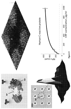
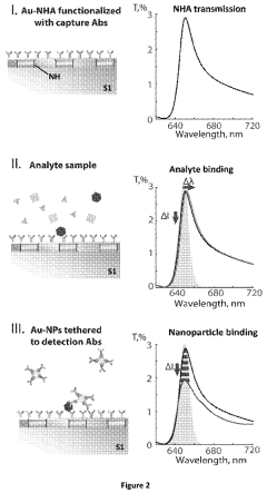
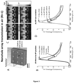
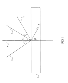
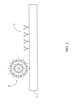
- A nanoparticle-enhanced plasmonic biosensor system using gold nano-hole arrays (Au-NHAs) that visualizes single sub-wavelength nanoparticles under bright-field imaging, enabling digital quantification and localization of individual nanoparticle-labeled molecules through local extraordinary optical transmission quenching, allowing for the detection of biomarkers at much lower concentrations, such as 10 pg/ml for biotinylated bovine serum albumin and 27 pg/ml for human C-reactive protein.
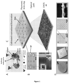
System and method for determining the presence or absence of adsorbed biomolecules or biomolecular structures on a surface
PatentInactiveUS20190056389A1
Innovation
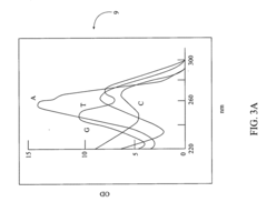
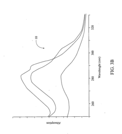
- The use of ultraviolet wavelengths to excite surface plasmons on a photonic surface with a diffraction grating, coinciding with native molecular absorption lines, and a thin aluminum layer with protective dielectric layers to enhance sensitivity and refractive index changes detection.
Nanofabrication Techniques for Plasmonic Biosensor Manufacturing
The fabrication of plasmonic biosensors for semiconductor applications requires sophisticated nanofabrication techniques that balance precision, scalability, and cost-effectiveness. Electron beam lithography (EBL) remains the gold standard for creating high-resolution plasmonic nanostructures with feature sizes below 10 nm. This technique offers exceptional control over pattern geometry but suffers from low throughput and high equipment costs, limiting its application primarily to research settings and prototype development.
Nanoimprint lithography (NIL) has emerged as a promising alternative, offering high-resolution patterning capabilities with significantly improved throughput compared to EBL. The technique involves creating a master template once using high-resolution methods, then replicating this pattern multiple times through mechanical embossing. This approach has demonstrated successful fabrication of plasmonic biosensors with feature sizes down to 20 nm while maintaining good uniformity across large areas.
Focused ion beam (FIB) milling provides another direct-write approach for creating plasmonic nanostructures. Unlike EBL, FIB allows for both material removal and deposition, enabling the fabrication of complex three-dimensional nanostructures. However, ion beam damage to surrounding areas can compromise the optical properties of plasmonic materials, necessitating careful process optimization.
Colloidal lithography offers a bottom-up approach to plasmonic biosensor fabrication. This technique utilizes self-assembled monolayers of nanospheres as templates or masks for subsequent material deposition. While lacking the precise geometric control of top-down approaches, colloidal lithography provides a cost-effective route to large-area fabrication of periodic nanostructure arrays with tunable optical properties.
Recent advances in directed self-assembly (DSA) combine the advantages of top-down and bottom-up approaches. By using pre-patterned substrates to guide the self-assembly of block copolymers, DSA enables the creation of highly ordered nanostructures with feature sizes below 10 nm across wafer-scale areas. This technique shows particular promise for high-volume manufacturing of plasmonic biosensors.
Metal deposition techniques also play a crucial role in plasmonic biosensor fabrication. Physical vapor deposition methods such as thermal evaporation and sputtering remain widely used, though chemical approaches including electroplating and electroless deposition offer advantages for creating complex geometries. Atomic layer deposition (ALD) has gained attention for its ability to create ultra-thin, conformal metal films with atomic-level thickness control, enabling precise tuning of plasmonic properties.
Surface functionalization represents the final critical step in biosensor manufacturing, where the plasmonic nanostructures are modified with biomolecular recognition elements. Techniques such as thiol-based self-assembled monolayers for gold surfaces and silane chemistry for oxide-coated surfaces provide robust platforms for subsequent attachment of antibodies, aptamers, or other biorecognition molecules.
Environmental and Biocompatibility Considerations for Semiconductor Biosensors
The integration of plasmonic biosensors into semiconductor applications necessitates careful consideration of environmental impacts and biocompatibility factors. These considerations are paramount as these devices increasingly interface with biological systems and environments, particularly in medical diagnostics and environmental monitoring applications.
Semiconductor-based plasmonic biosensors typically incorporate various materials including noble metals (gold, silver), semiconductor substrates (silicon, gallium arsenide), and functional coatings. The environmental footprint of these materials spans their entire lifecycle—from extraction and processing to disposal. Noble metals used in plasmonic structures require energy-intensive mining and refining processes that generate significant carbon emissions and can lead to habitat disruption.
Manufacturing processes for semiconductor biosensors involve potentially hazardous chemicals such as photoresists, etchants, and solvents. These substances can pose environmental risks if not properly managed through waste treatment systems. Additionally, cleanroom operations demand substantial energy consumption, contributing to the overall environmental impact of these devices.
Biocompatibility represents another critical dimension for plasmonic biosensor development. When these sensors interface with biological samples or are deployed in vivo, they must not elicit adverse biological responses. Gold nanostructures generally exhibit good biocompatibility, whereas silver nanoparticles may release ions that demonstrate cytotoxic effects. Surface functionalization strategies must be carefully selected to maintain sensor performance while ensuring biological safety.
Recent advances have focused on developing more sustainable approaches to plasmonic biosensor fabrication. These include the exploration of alternative plasmonic materials such as aluminum and copper, which offer lower environmental impact compared to traditional noble metals. Researchers are also investigating biodegradable substrates and green chemistry approaches to reduce the environmental footprint of manufacturing processes.
Regulatory frameworks governing the environmental and biocompatibility aspects of semiconductor biosensors continue to evolve. The FDA in the United States and similar bodies internationally have established guidelines for biocompatibility testing of medical devices, which increasingly apply to advanced biosensing technologies. ISO 10993 standards provide protocols for evaluating biological responses to materials used in medical devices, including potential cytotoxicity, sensitization, and systemic toxicity.
End-of-life considerations for semiconductor biosensors present unique challenges due to their hybrid nature, combining electronic components with biological recognition elements. Developing effective recycling strategies for these complex devices remains an active area of research, with particular focus on recovering precious metals while safely disposing of potentially biohazardous materials.
Unlock deeper insights with Patsnap Eureka Quick Research — get a full tech report to explore trends and direct your research. Try now!
Generate Your Research Report Instantly with AI Agent
Supercharge your innovation with Patsnap Eureka AI Agent Platform!