Silicon Micropillars in Nanopositioning Devices
JUL 9, 202510 MIN READ
Generate Your Research Report Instantly with AI Agent
Patsnap Eureka helps you evaluate technical feasibility & market potential.
Silicon Micropillar Background and Objectives
Silicon micropillars have emerged as a crucial component in the field of nanopositioning devices, revolutionizing precision control and measurement at the nanoscale. The development of these structures can be traced back to the early 2000s when researchers began exploring novel approaches to enhance the performance of micro-electromechanical systems (MEMS). The evolution of silicon micropillars has been driven by the increasing demand for higher precision and stability in various applications, including atomic force microscopy, semiconductor manufacturing, and biomedical imaging.
The primary objective of research on silicon micropillars in nanopositioning devices is to achieve unprecedented levels of accuracy, resolution, and repeatability in positioning and motion control at the nanometer scale. This technology aims to overcome the limitations of traditional positioning systems, which often struggle with issues such as thermal drift, mechanical instability, and insufficient precision for cutting-edge applications.
Silicon micropillars offer several advantages that make them particularly suitable for nanopositioning applications. Their high aspect ratio and mechanical properties allow for the creation of structures that are both flexible and robust, capable of withstanding the forces involved in nanoscale movements while maintaining exceptional stability. Additionally, the use of silicon as the base material enables seamless integration with existing semiconductor fabrication processes, facilitating mass production and cost-effectiveness.
The development of silicon micropillars for nanopositioning devices has been marked by continuous improvements in design, fabrication techniques, and integration methods. Early research focused on optimizing the geometry and dimensions of these structures to achieve the desired mechanical properties. Subsequent efforts have explored various surface treatments and coatings to enhance performance and durability.
Recent technological trends in this field include the incorporation of advanced sensing and actuation mechanisms directly into the micropillar structures, creating integrated nanopositioning systems with enhanced functionality. Researchers are also investigating the potential of hybrid materials and novel fabrication techniques to further improve the performance and versatility of silicon micropillar-based devices.
As the field progresses, the objectives of silicon micropillar research in nanopositioning devices continue to evolve. Current goals include achieving sub-nanometer positioning accuracy, expanding the range of motion while maintaining precision, and developing multi-axis positioning systems capable of complex movements in three-dimensional space. Additionally, there is a growing emphasis on improving the long-term stability and reliability of these devices, as well as reducing their power consumption and overall footprint.
The future of silicon micropillars in nanopositioning devices holds great promise for enabling groundbreaking advancements in various scientific and technological domains. As research in this area continues to advance, it is expected to drive innovation in fields such as quantum computing, advanced microscopy, and nanoscale manufacturing, ultimately contributing to the development of next-generation technologies that require unprecedented levels of precision and control.
Nanopositioning Market Analysis
The nanopositioning market has experienced significant growth in recent years, driven by increasing demand for high-precision positioning systems across various industries. This market segment is closely tied to the development and implementation of silicon micropillars in nanopositioning devices, which offer enhanced performance and accuracy.
The global nanopositioning market is primarily fueled by the semiconductor industry, where precise positioning is crucial for manufacturing processes such as lithography, inspection, and metrology. As chip manufacturers continue to push the boundaries of miniaturization, the need for more accurate and stable nanopositioning systems becomes paramount.
Beyond semiconductors, other key sectors contributing to market growth include life sciences, aerospace, and advanced manufacturing. In life sciences, nanopositioning systems are essential for applications like DNA sequencing, cell manipulation, and high-resolution microscopy. The aerospace industry utilizes these systems for satellite communication and optical systems alignment. Advanced manufacturing benefits from nanopositioning in areas such as 3D printing, laser cutting, and precision assembly.
The adoption of silicon micropillars in nanopositioning devices has opened new opportunities in the market. These structures offer improved stability, reduced thermal drift, and enhanced vibration isolation compared to traditional positioning systems. As a result, industries requiring ultra-high precision are increasingly turning to silicon micropillar-based solutions.
Market trends indicate a growing preference for multi-axis nanopositioning systems that can provide simultaneous control in multiple degrees of freedom. This trend aligns well with the capabilities of silicon micropillar arrays, which can be designed to offer complex motion profiles in compact form factors.
Geographically, North America and Asia-Pacific lead the nanopositioning market, with Europe following closely. The Asia-Pacific region, particularly countries like China, Japan, and South Korea, is expected to see the fastest growth due to their strong presence in semiconductor manufacturing and increasing investments in research and development.
The competitive landscape of the nanopositioning market is characterized by a mix of established players and innovative startups. Key market players are focusing on developing integrated solutions that combine advanced control algorithms with silicon micropillar hardware to offer superior performance and ease of use.
Looking ahead, the nanopositioning market is poised for continued expansion, with projections suggesting steady growth over the next decade. Factors such as the increasing complexity of nanotechnology applications, the rise of quantum technologies, and the push towards Industry 4.0 are expected to drive demand for more sophisticated nanopositioning solutions, including those based on silicon micropillar technology.
Current Challenges in Micropillar Fabrication
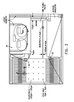
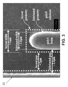
The fabrication of silicon micropillars for nanopositioning devices presents several significant challenges that researchers and engineers must overcome. One of the primary difficulties lies in achieving precise dimensional control and uniformity across large arrays of micropillars. The high aspect ratio of these structures, often exceeding 10:1, makes it challenging to maintain consistent pillar height and diameter throughout the fabrication process.
Etching techniques, such as deep reactive ion etching (DRIE), are commonly employed to create micropillars. However, these methods can lead to issues like scalloping on the pillar sidewalls, which affects the overall pillar geometry and performance. Additionally, the etch rate may vary across the wafer, resulting in non-uniform pillar heights. Controlling these factors becomes increasingly difficult as the pillar dimensions decrease and the array size increases.
Another significant challenge is the prevention of pillar collapse during the fabrication and subsequent processing steps. As the aspect ratio of the pillars increases, they become more susceptible to bending and sticking to neighboring pillars or the substrate surface due to capillary forces during wet processing or surface tension effects. This phenomenon, known as stiction, can severely impact the functionality and yield of the nanopositioning devices.
The choice of materials and their properties also present challenges in micropillar fabrication. While silicon is a popular choice due to its well-established processing techniques, it may not always provide the optimal mechanical or electrical properties required for specific nanopositioning applications. Exploring alternative materials or creating composite structures often introduces additional complexities in the fabrication process.
Surface roughness and pillar tip geometry are critical factors that affect the performance of nanopositioning devices. Achieving atomically smooth surfaces and well-defined pillar tips at the nanoscale remains a significant challenge. Techniques such as oxidation sharpening or focused ion beam milling can be employed to refine the pillar tips, but these processes add complexity and may introduce variability in the final structures.
Integration of micropillars with other components of nanopositioning devices, such as actuators and sensors, presents another set of challenges. Ensuring proper alignment, electrical connections, and mechanical coupling between the micropillars and other device elements requires precise control and often necessitates the development of novel fabrication and assembly techniques.
Scalability and reproducibility of the fabrication process are crucial for the commercial viability of micropillar-based nanopositioning devices. Developing processes that can consistently produce high-quality micropillars over large areas and across multiple wafers remains a significant challenge, particularly as the demand for higher-density arrays and more complex device architectures increases.
Existing Micropillar Fabrication Techniques
01 Micropillar fabrication techniques
Various techniques are employed to fabricate silicon micropillars with high positioning accuracy. These methods include lithography, etching processes, and advanced deposition techniques. The precise control of these fabrication processes is crucial for achieving accurate positioning of micropillars on silicon substrates.- Micropillar fabrication techniques: Various techniques are employed to fabricate silicon micropillars with high positioning accuracy. These methods include photolithography, etching processes, and advanced deposition techniques. The precise control of these fabrication processes is crucial for achieving accurate positioning of the micropillars on the substrate.
- Alignment and calibration systems: Specialized alignment and calibration systems are used to ensure accurate positioning of silicon micropillars. These systems often incorporate advanced optical or mechanical methods to align the micropillars with high precision. Calibration techniques are employed to maintain accuracy over time and compensate for any drift or environmental factors.
- Positioning control mechanisms: Various control mechanisms are implemented to achieve precise positioning of silicon micropillars. These may include piezoelectric actuators, micromanipulators, or other high-precision positioning devices. Feedback systems are often integrated to continuously monitor and adjust the position of the micropillars.
- Measurement and characterization techniques: Advanced measurement and characterization techniques are employed to assess the positioning accuracy of silicon micropillars. These may include high-resolution imaging methods, interferometry, or scanning probe microscopy. The data obtained from these measurements is used to validate and improve the positioning accuracy.
- Integration with other microstructures: Methods for integrating silicon micropillars with other microstructures while maintaining positioning accuracy are developed. This includes techniques for combining micropillars with microfluidic channels, sensors, or other functional elements on the same substrate. The integration process must preserve the precise positioning of the micropillars within the larger system.
02 Alignment and positioning systems
Advanced alignment and positioning systems are utilized to ensure accurate placement of silicon micropillars. These systems often incorporate high-precision actuators, sensors, and feedback mechanisms to achieve nanometer-scale positioning accuracy. Computer-controlled positioning stages and interferometric measurement techniques are commonly employed.Expand Specific Solutions03 Optical measurement and characterization
Optical measurement techniques play a crucial role in verifying and improving the positioning accuracy of silicon micropillars. These methods include interferometry, confocal microscopy, and advanced imaging systems. Real-time monitoring and feedback during fabrication processes help maintain high positioning accuracy.Expand Specific Solutions04 Integration with microelectronics
Silicon micropillars are often integrated with microelectronic devices to enhance functionality. Precise positioning is critical for ensuring proper electrical connections and device performance. Advanced packaging techniques and interconnect technologies are employed to maintain positioning accuracy during integration processes.Expand Specific Solutions05 Environmental control and stability
Maintaining environmental stability is crucial for achieving high positioning accuracy of silicon micropillars. Vibration isolation systems, temperature control, and clean room environments are utilized to minimize external factors that could affect positioning accuracy. Advanced materials and designs are also employed to enhance the structural stability of micropillar arrays.Expand Specific Solutions
Key Players in Micropillar Industry
The research on silicon micropillars in nanopositioning devices is in an emerging stage, with significant potential for growth. The market size is expanding as demand increases for high-precision positioning in various industries. Technologically, it's progressing from early development to more advanced applications. Key players like Massachusetts Institute of Technology, California Institute of Technology, and NXP Semiconductors are driving innovation. Universities such as Technische Universität Ilmenau and Harbin Institute of Technology are contributing to fundamental research. Companies like Corning and Nanosys are exploring commercial applications. The involvement of diverse institutions indicates a competitive landscape with opportunities for breakthroughs in both academic and industrial sectors.
Technische Universität Ilmenau
Technical Solution: Technische Universität Ilmenau has developed a unique approach to silicon micropillars in nanopositioning devices, focusing on high-speed operation and thermal stability. Their design incorporates an array of silicon micropillars with integrated thermoelectric elements, allowing for rapid and precise temperature control. The micropillars are fabricated using a combination of deep reactive ion etching and selective epitaxial growth, resulting in structures with high aspect ratios and excellent mechanical properties [10]. The nanopositioning system utilizes a novel actuation mechanism combining electrostatic and thermal effects, enabling fast response times in the microsecond range [11]. Additionally, the university has implemented an advanced feedback control system that compensates for thermal drift in real-time, ensuring consistent performance across a wide temperature range. The device also features an innovative optical sensing system using integrated waveguides within the micropillar structure for high-precision position monitoring [12].
Strengths: High-speed operation, excellent thermal stability, and innovative integration of multiple physical effects for precise control. Weaknesses: Potential energy consumption issues due to active thermal management and complexity in fabrication process.
Cambridge Enterprise Ltd.
Technical Solution: Cambridge Enterprise has developed an innovative approach to silicon micropillars in nanopositioning devices, focusing on scalability and integration with existing semiconductor manufacturing processes. Their design utilizes a hierarchical structure of silicon micropillars, with larger pillars for coarse positioning and smaller, nested pillars for fine adjustments. The fabrication process employs a combination of standard CMOS techniques and advanced etching methods, allowing for mass production compatibility [13]. The nanopositioning system incorporates a novel electromagnetic actuation mechanism, with micro-coils integrated into the silicon substrate, enabling precise control of individual micropillars [14]. Cambridge's design also features an on-chip capacitive sensing array for real-time position feedback, achieving nanometer-scale resolution. Additionally, they have developed a unique surface treatment process for the micropillars, enhancing wear resistance and reducing stiction effects in long-term operation [15].
Strengths: High scalability, compatibility with existing semiconductor manufacturing processes, and innovative hierarchical design for multi-scale positioning. Weaknesses: Potential limitations in achieving ultra-high precision compared to more specialized approaches and challenges in electromagnetic shielding for sensitive applications.
Core Innovations in Silicon Micropillars
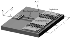
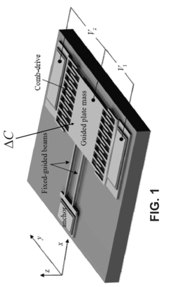
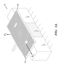
Monolithic Comb Drive System and method for Large-Deflection Multi-Dof Microtransduction
PatentInactiveUS20100064395A1
Innovation
- The Electro Micro-Metrology (EMM) method leverages sensitive electrical-mechanical coupling to measure and characterize micro/nanoscale properties using electrical measurands such as capacitance, voltage, and frequency, enabling precise calibration and characterization of geometric, dynamic, and material properties with improved accuracy and reliability.
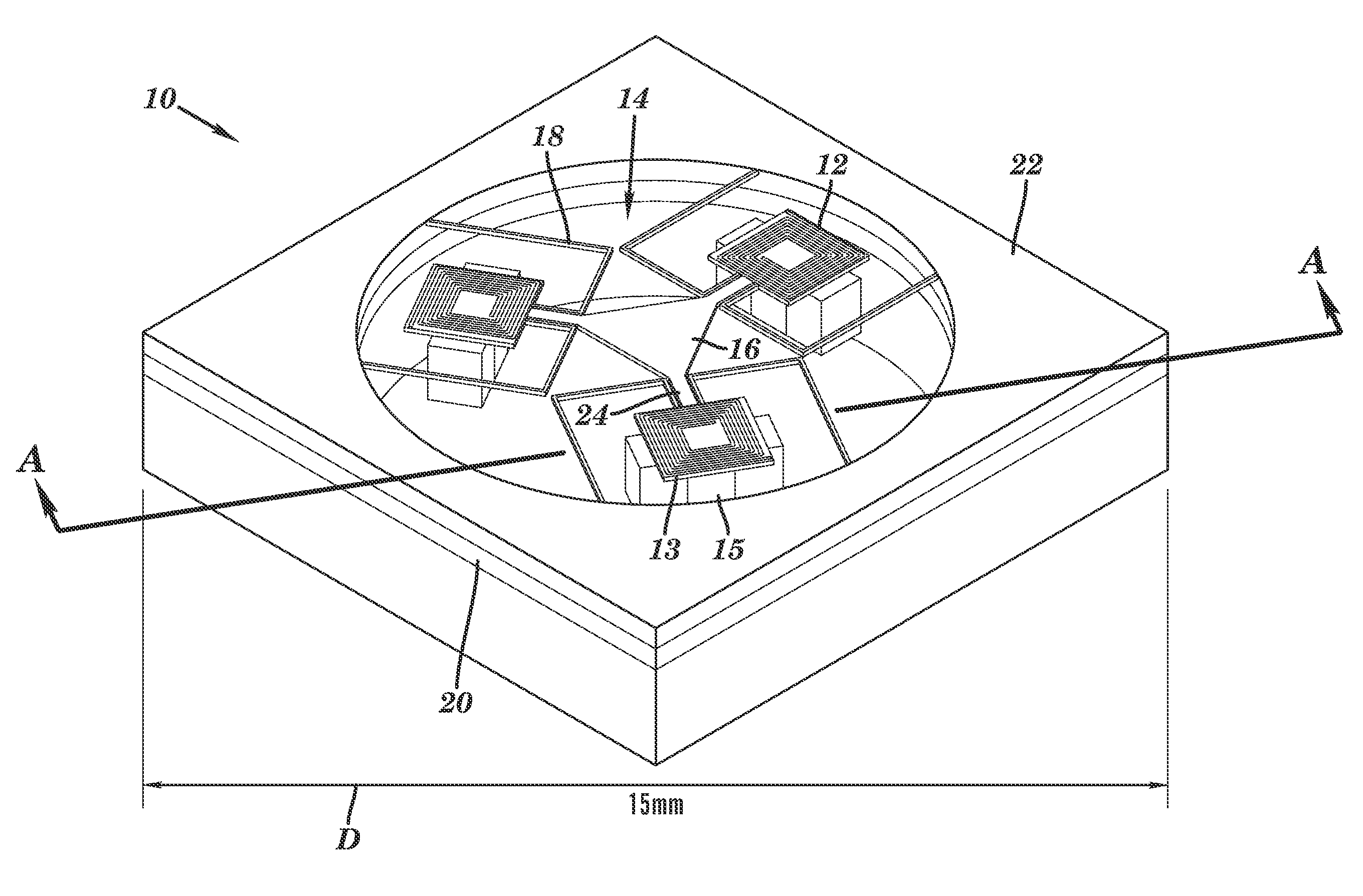
6-axis electromagnetically-actuated meso-scale nanopositioner
PatentInactiveUS7557470B2
Innovation
- A microfabricated nanopositioner with a compliant mechanism and microfabricated actuators featuring a coil stack of electrically conductive superposed layers and a magnet array, allowing for controlled movement in six degrees of freedom through in-plane and out-of-plane actuation, with thermal error correction to minimize position errors.
Materials Science Advancements
Recent advancements in materials science have significantly contributed to the development of silicon micropillars for nanopositioning devices. The unique properties of silicon, including its high strength-to-weight ratio, excellent thermal conductivity, and compatibility with existing semiconductor fabrication processes, make it an ideal material for these applications. Researchers have made substantial progress in optimizing the structural and mechanical properties of silicon micropillars to enhance their performance in nanopositioning systems.
One key area of advancement has been the refinement of fabrication techniques for silicon micropillars. Improved etching processes, such as deep reactive ion etching (DRIE) and focused ion beam (FIB) milling, have enabled the creation of high-aspect-ratio micropillars with precise dimensions and smooth surfaces. These techniques allow for better control over the pillar geometry, which is crucial for achieving the desired mechanical properties and performance characteristics in nanopositioning devices.
Surface modification of silicon micropillars has also seen significant progress. Researchers have developed various methods to functionalize the pillar surfaces, including chemical vapor deposition (CVD) and atomic layer deposition (ALD). These techniques allow for the deposition of thin films or nanoparticles on the micropillar surfaces, enhancing their mechanical, electrical, or optical properties. Such modifications can improve the sensitivity and accuracy of nanopositioning devices by optimizing the interaction between the micropillars and the surrounding environment.
The integration of novel materials with silicon micropillars has opened up new possibilities for enhancing device performance. For instance, the incorporation of piezoelectric materials, such as lead zirconate titanate (PZT) or aluminum nitride (AlN), into silicon micropillar structures has enabled the development of highly responsive actuators for nanopositioning applications. These hybrid structures combine the mechanical stability of silicon with the precise control offered by piezoelectric materials, resulting in improved positioning accuracy and faster response times.
Advancements in characterization techniques have also played a crucial role in understanding and optimizing the behavior of silicon micropillars. High-resolution imaging methods, such as scanning electron microscopy (SEM) and transmission electron microscopy (TEM), allow researchers to analyze the microstructure and defects in micropillars with unprecedented detail. Additionally, advanced mechanical testing techniques, including nanoindentation and in-situ TEM mechanical testing, provide valuable insights into the deformation mechanisms and failure modes of silicon micropillars under various loading conditions.
Nanopositioning Device Applications
Nanopositioning devices have found widespread applications across various fields, revolutionizing precision control and measurement at the nanoscale. In the semiconductor industry, these devices play a crucial role in lithography processes, enabling the fabrication of increasingly smaller and more complex integrated circuits. The ability to position wafers and photomasks with nanometer-level accuracy is essential for achieving high-resolution patterns and maintaining yield in chip manufacturing.
In the field of microscopy, nanopositioning devices have significantly enhanced imaging capabilities. Scanning probe microscopes, such as atomic force microscopes (AFM) and scanning tunneling microscopes (STM), rely on precise positioning of probes to generate high-resolution images of surfaces at the atomic scale. These devices allow researchers to study material properties, surface topography, and molecular structures with unprecedented detail.
The biomedical sector has also benefited greatly from nanopositioning technology. In applications such as cell manipulation and drug delivery, nanopositioning devices enable precise control over the placement of microscopic objects or the administration of therapeutic agents. This level of accuracy is particularly valuable in single-cell analysis, where researchers can study individual cells' behavior and responses to stimuli.
In the field of optics and photonics, nanopositioning devices are essential for aligning optical components with sub-wavelength precision. This capability is crucial for developing advanced optical systems, such as laser-based instruments, fiber optic communication networks, and quantum optical devices. The ability to fine-tune optical elements at the nanoscale has led to improvements in spectroscopy, interferometry, and other light-based measurement techniques.
Nanopositioning devices have also found applications in the aerospace and defense industries. They are used in the development of high-precision gyroscopes and accelerometers, which are critical components in navigation systems and inertial measurement units. The enhanced accuracy provided by nanopositioning technology contributes to improved guidance and control systems for aircraft, satellites, and other aerospace vehicles.
In materials science and nanotechnology research, nanopositioning devices enable the manipulation and characterization of nanomaterials. They are used in nanoindentation experiments to study mechanical properties of materials at the nanoscale, as well as in the assembly of nanostructures for novel device fabrication. This capability has opened up new avenues for developing advanced materials with tailored properties for specific applications.
As the demand for miniaturization and precision continues to grow across industries, the applications of nanopositioning devices are expected to expand further. The integration of silicon micropillars in these devices holds promise for enhancing their performance and enabling new functionalities, potentially leading to breakthroughs in various fields that rely on nanoscale precision and control.
Unlock deeper insights with Patsnap Eureka Quick Research — get a full tech report to explore trends and direct your research. Try now!
Generate Your Research Report Instantly with AI Agent
Supercharge your innovation with Patsnap Eureka AI Agent Platform!