Scaling Thermoelectric Generators In Semiconductor Manufacturing
SEP 12, 20259 MIN READ
Generate Your Research Report Instantly with AI Agent
Patsnap Eureka helps you evaluate technical feasibility & market potential.
TEG Technology Background and Objectives
Thermoelectric generators (TEGs) represent a significant technological advancement in energy harvesting, converting waste heat directly into electrical energy through the Seebeck effect. The concept dates back to the early 19th century, but its integration into semiconductor manufacturing processes has gained momentum only in recent decades. This evolution has been driven by increasing demands for energy efficiency, miniaturization of electronic devices, and sustainable power solutions in various industries.
The semiconductor industry has traditionally focused on improving computational power and reducing energy consumption. However, the inevitable heat generation during semiconductor operation presents both a challenge and an opportunity. TEGs offer a promising solution by capturing this waste heat and converting it into usable electrical energy, thereby improving overall system efficiency.
Recent technological advancements in material science, particularly in the development of high-performance thermoelectric materials with improved figure of merit (ZT), have significantly enhanced the efficiency and applicability of TEGs. These materials include bismuth telluride (Bi2Te3), lead telluride (PbTe), and silicon-germanium alloys (SiGe), each optimized for different temperature ranges and applications.
The integration of TEGs into semiconductor manufacturing processes presents unique scaling challenges. Traditional TEG fabrication methods often involve bulk materials and processes incompatible with standard semiconductor manufacturing techniques. The objective is to develop scalable TEG technologies that can be seamlessly integrated into existing semiconductor manufacturing processes, enabling mass production of efficient, cost-effective thermoelectric solutions.
Key technical objectives include enhancing the power density of TEGs to make them viable for a wider range of applications, improving thermal management to maximize temperature differentials, and developing novel materials and structures that can be fabricated using standard semiconductor processes. Additionally, there is a focus on reducing the cost per watt of TEG technology to make it economically competitive with other energy harvesting methods.
The environmental impact of TEG technology also forms a critical aspect of its development trajectory. By converting waste heat into electricity, TEGs can contribute to reducing greenhouse gas emissions and improving energy efficiency across various sectors, aligning with global sustainability goals.
Looking forward, the scaling of TEGs in semiconductor manufacturing aims to enable a new generation of self-powered electronic devices, from wearable technology to Internet of Things (IoT) sensors, and to enhance energy recovery in industrial processes, automotive applications, and consumer electronics. This technology holds the potential to transform how we think about energy usage and recovery in electronic systems.
Market Analysis for Semiconductor-Based TEGs
The global market for semiconductor-based Thermoelectric Generators (TEGs) is experiencing significant growth, driven by increasing demand for energy harvesting solutions across multiple industries. Current market valuations place the semiconductor TEG sector at approximately 460 million USD in 2023, with projections indicating a compound annual growth rate of 8.2% through 2030, potentially reaching 790 million USD by the end of the decade.
The automotive sector represents the largest application market for semiconductor TEGs, accounting for roughly 32% of total market share. This dominance stems from the automotive industry's push toward greater fuel efficiency and reduced emissions, with TEGs offering a viable solution for converting waste heat from exhaust systems into usable electrical power. Major automotive manufacturers including BMW, Ford, and Toyota have initiated research programs to integrate TEG technology into their vehicle designs.
Consumer electronics constitutes the second-largest market segment at 24%, where miniaturized TEGs are being developed for wearable devices, IoT sensors, and portable electronics. The appeal in this sector lies in the potential for self-powered devices that can operate without battery replacement, significantly extending operational lifespans and reducing maintenance requirements.
Industrial applications represent a rapidly growing segment (18% market share), particularly in manufacturing environments where waste heat recovery can substantially improve energy efficiency metrics. The remaining market share is distributed across aerospace (12%), medical devices (8%), and other applications (6%).
Geographically, North America leads the market with approximately 38% share, followed by Europe (29%) and Asia-Pacific (26%). However, the Asia-Pacific region is expected to demonstrate the highest growth rate over the next five years, driven by expanding semiconductor manufacturing capabilities in China, South Korea, and Taiwan, coupled with increasing industrial automation.
Key market drivers include the global push for energy efficiency, stringent environmental regulations, and the growing Internet of Things ecosystem requiring distributed power sources. The increasing focus on sustainable energy solutions has positioned semiconductor TEGs as an attractive technology for capturing otherwise wasted thermal energy.
Market challenges primarily revolve around efficiency limitations, with current commercial semiconductor TEGs typically operating at 5-8% conversion efficiency. Cost factors also remain significant, as specialized semiconductor materials and precision manufacturing processes contribute to relatively high production expenses compared to alternative energy technologies.
The competitive landscape features established semiconductor manufacturers like Analog Devices and Texas Instruments alongside specialized thermoelectric companies such as Ferrotec and Laird Thermal Systems. Recent market entrants include several technology startups focused on novel materials and manufacturing techniques to improve TEG performance and reduce costs.
Current Challenges in TEG Scaling
Despite significant advancements in thermoelectric generator (TEG) technology, scaling these devices for semiconductor manufacturing presents several formidable challenges. The fundamental issue lies in maintaining high thermoelectric efficiency while reducing device dimensions to meet semiconductor industry standards. Current TEG designs struggle to deliver adequate power density when miniaturized, creating a significant barrier to widespread integration.
Material compatibility represents another major obstacle. Traditional thermoelectric materials like bismuth telluride and lead telluride contain elements that are considered contaminants in standard semiconductor processes. This incompatibility necessitates isolation techniques or alternative material development, both of which add complexity and cost to manufacturing processes.
Thermal management becomes increasingly problematic at smaller scales. As TEGs shrink, the thermal interface between hot and cold sides becomes more difficult to maintain, resulting in reduced temperature gradients and consequently lower power output. Heat dissipation mechanisms that work effectively at larger scales often fail to perform adequately when miniaturized to semiconductor dimensions.
Manufacturing precision presents another significant challenge. TEG performance is highly sensitive to dimensional variations, with even minor inconsistencies potentially causing substantial efficiency losses. Current semiconductor manufacturing techniques struggle to consistently produce thermoelectric elements with the required precision at scale, particularly when dealing with complex three-dimensional structures necessary for optimal TEG performance.
Cost considerations further complicate scaling efforts. While semiconductor manufacturing benefits from economies of scale, thermoelectric materials remain relatively expensive, and the additional processing steps required for TEG integration can significantly increase production costs. This economic barrier has limited commercial adoption despite the technology's potential benefits.
Integration with existing semiconductor processes represents perhaps the most immediate challenge. TEGs typically require specialized fabrication steps that are not standard in semiconductor manufacturing lines. Adapting these processes for compatibility with high-volume semiconductor production while maintaining performance specifications has proven exceptionally difficult.
Reliability and longevity concerns also persist. Thermal cycling in semiconductor applications can accelerate degradation of thermoelectric materials, particularly at interface regions. Current TEG designs often demonstrate performance deterioration over time when subjected to the operational conditions typical in semiconductor environments, limiting their practical lifespan and reliability.
Current Scaling Solutions for TEGs
01 Miniaturization and scaling of thermoelectric generators
Thermoelectric generators can be scaled down to micro and nano dimensions to improve efficiency and power density. Miniaturization techniques allow for the development of compact thermoelectric devices suitable for integration into small electronic systems. These scaled-down generators can harvest waste heat from various sources while maintaining a small footprint, making them ideal for portable and wearable applications.- Miniaturization and scaling of thermoelectric generators: Advancements in miniaturization techniques allow for the scaling down of thermoelectric generators while maintaining or improving efficiency. These scaled-down generators can be integrated into smaller devices and applications. The miniaturization process involves specialized fabrication methods that preserve the thermoelectric properties at reduced dimensions, enabling more compact power generation solutions for portable and wearable electronics.
- Material innovations for improved thermoelectric performance: Novel materials and composites are being developed to enhance the efficiency of thermoelectric generators at various scales. These materials exhibit improved Seebeck coefficients, electrical conductivity, and reduced thermal conductivity, which are crucial for efficient energy conversion. Advanced semiconductor materials, nanostructured compounds, and organic-inorganic hybrids are being utilized to optimize the figure of merit (ZT) across different operating temperatures and scales.
- Structural design optimization for scalable thermoelectric systems: Innovative structural designs are being implemented to optimize the performance of thermoelectric generators at different scales. These designs focus on maximizing the temperature gradient across the thermoelectric elements while minimizing thermal losses. Various geometrical configurations, including stacked, cascaded, and radial arrangements, are being explored to enhance power output and efficiency as the systems scale up or down in size.
- Integration techniques for thermoelectric generators in various applications: Advanced integration methods are being developed to incorporate thermoelectric generators into diverse applications at different scales. These techniques address challenges related to thermal management, electrical connections, and mechanical stability. The integration approaches enable thermoelectric generators to be effectively deployed in automotive systems, industrial waste heat recovery, consumer electronics, and even microscale biomedical devices.
- Manufacturing processes for scalable production: Innovative manufacturing techniques are being developed to enable cost-effective and scalable production of thermoelectric generators. These processes include advanced deposition methods, printing technologies, and automated assembly techniques that maintain precise control over material properties and device geometry. The manufacturing approaches allow for both mass production of standardized modules and customized fabrication of application-specific thermoelectric generators across various size scales.
02 Material innovations for improved thermoelectric performance
Advanced materials are being developed to enhance the efficiency of thermoelectric generators at different scales. These include nanostructured materials, semiconductor alloys, and composite materials that exhibit improved Seebeck coefficients and reduced thermal conductivity. Material innovations focus on increasing the figure of merit (ZT) to achieve better energy conversion efficiency across various operating temperatures and device scales.Expand Specific Solutions03 Modular and stackable thermoelectric generator designs
Modular approaches to thermoelectric generator design allow for scalable power output by connecting multiple units in series or parallel configurations. These stackable designs enable customization of voltage, current, and power output based on application requirements. The modular architecture facilitates easy maintenance, replacement of individual components, and adaptation to different heat source geometries and thermal gradients.Expand Specific Solutions04 Integration of thermoelectric generators with other energy systems
Thermoelectric generators can be integrated with other energy harvesting or generation systems to create hybrid solutions that maximize overall efficiency. These integrated approaches combine thermoelectric technology with solar panels, fuel cells, or mechanical energy harvesters to provide complementary power generation capabilities. The scaling of these integrated systems allows for deployment across various applications from small wearable devices to larger industrial waste heat recovery systems.Expand Specific Solutions05 Fabrication techniques for mass production of thermoelectric generators
Advanced manufacturing methods enable the mass production of thermoelectric generators at various scales. These techniques include thin-film deposition, printing technologies, microfabrication processes, and automated assembly methods that reduce production costs while maintaining performance. Scalable fabrication approaches are essential for the commercial viability of thermoelectric generators in consumer electronics, automotive applications, and industrial waste heat recovery systems.Expand Specific Solutions
Key Industry Players in TEG Manufacturing
The thermoelectric generator (TEG) market in semiconductor manufacturing is currently in a growth phase, with increasing adoption driven by energy efficiency demands. The global market size is projected to expand significantly as applications diversify across automotive, industrial, and consumer electronics sectors. Technologically, the field shows varying maturity levels, with companies like Toyota, Infineon, and GLOBALFOUNDRIES leading commercial implementation, while Guangdong Fuxin Technology and Hangzhou Dahe Thermo-Magnetics demonstrate strong specialization in thermoelectric solutions. Research institutions including Technical Institute of Physics & Chemistry CAS and University of Washington are advancing fundamental innovations. Semiconductor giants such as TSMC, Samsung, and STMicroelectronics are integrating TEG technologies into their manufacturing processes, focusing on scaling challenges and efficiency improvements to meet growing demand for energy harvesting solutions in next-generation semiconductor devices.
Toyota Motor Corp.
Technical Solution: Toyota has developed a comprehensive approach to scaling thermoelectric generators for automotive applications, with particular focus on exhaust heat recovery systems. Their manufacturing technology centers on segmented thermoelectric modules that can operate efficiently across the wide temperature ranges found in vehicle exhaust systems (200-600°C). Toyota's process incorporates specialized high-temperature materials like half-Heusler alloys and skutterudites for hot-side operation, transitioning to bismuth telluride compounds for lower temperature regions. Their manufacturing approach includes precision casting and powder metallurgy techniques to create bulk thermoelectric elements with controlled microstructures that reduce thermal conductivity while maintaining electrical performance. Toyota has pioneered hermetic packaging technologies that protect thermoelectric materials from oxidation and sublimation at high temperatures while withstanding severe thermal cycling. Their integration strategy includes specialized heat exchangers designed to maximize temperature differentials across the TEG modules while minimizing exhaust flow restrictions. Toyota has demonstrated these systems in production vehicles, achieving power generation of up to 200W under highway driving conditions, directly contributing to reduced fuel consumption and emissions.
Strengths: Extensive real-world validation in automotive environments; excellent durability under thermal cycling and vibration; comprehensive system integration approach including cooling and power conditioning; scalable manufacturing processes. Weaknesses: Relatively high system complexity increases installation and maintenance costs; performance dependent on driving conditions and ambient temperatures; challenges in material durability at highest operating temperatures.
Stmicroelectronics Srl
Technical Solution: STMicroelectronics has developed an innovative approach to scaling thermoelectric generators through their "Smart TEG" platform, which integrates thermoelectric materials directly with microcontroller and sensor technologies. Their manufacturing process leverages existing MEMS fabrication capabilities to create miniaturized TEG structures with thousands of thermocouples in series. ST's technology utilizes specialized bismuth telluride and antimony telluride compounds optimized for room-temperature operation, with proprietary doping profiles that enhance carrier mobility while reducing thermal conductivity. Their manufacturing approach includes wafer-level bonding techniques to create vacuum-sealed TEG modules that minimize convective heat losses and maximize temperature differentials. ST has pioneered the integration of these TEG modules with ultra-low-power microcontrollers from their STM32 family, creating self-powered sensor nodes for IoT applications. Their process includes deposition of specialized thermal interface materials that direct heat flow optimally through the thermoelectric elements. ST has demonstrated successful integration of these TEG solutions in industrial monitoring systems, achieving power densities of up to 30μW/cm² with temperature differentials of just 10°C.
Strengths: Excellent integration with microcontroller and sensor ecosystems; highly miniaturized form factors suitable for IoT applications; established manufacturing infrastructure; comprehensive power management solutions. Weaknesses: Limited power output compared to larger TEG systems; challenges in thermal management at very small scales; higher cost per watt than conventional power sources for IoT devices.
Critical Patents in TEG Semiconductor Integration
Manufacturing process of the thermoelectric conversion element
PatentInactiveUS20160035958A1
Innovation
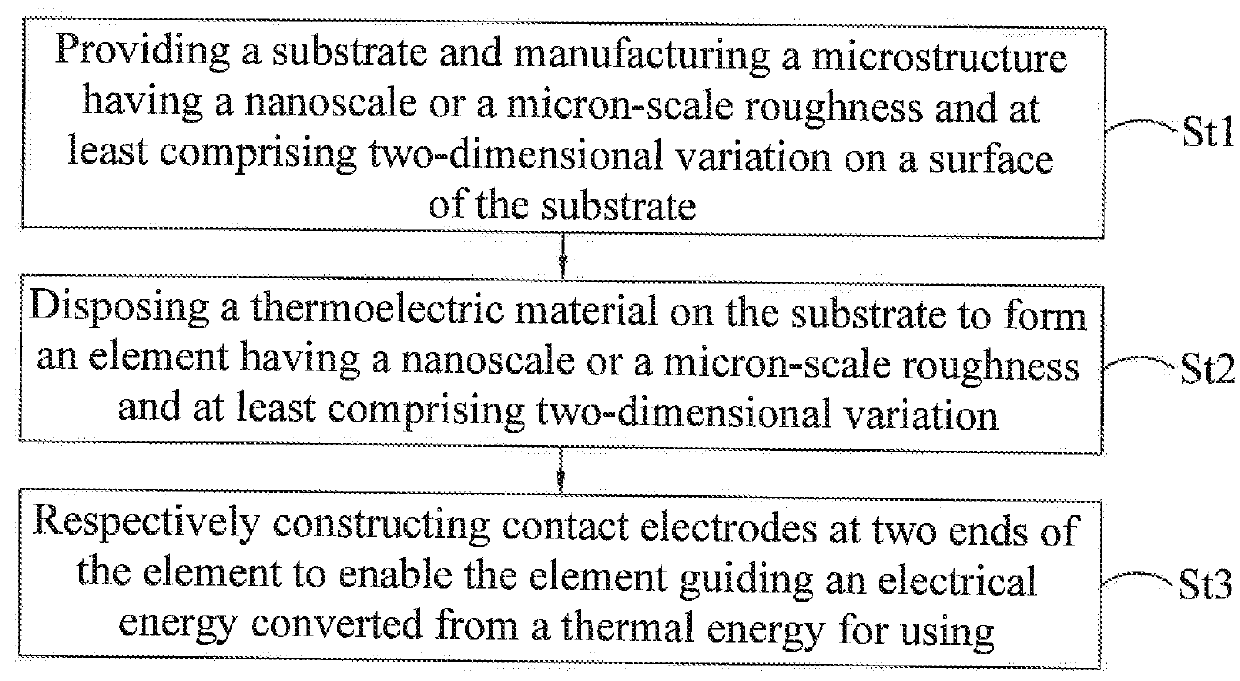
- A manufacturing process that creates a thermoelectric conversion element with a nanoscale or microscale structure using a semiconductor manufacturing technique, which increases carrier scattering and maintains high temperature differences while reducing thermal conductivity, allowing for improved thermoelectric figure of merit without affecting thermal conductivity.
MEMS thermoelectric generator, manufacturing process of the generator and heating system comprising the generator
PatentActiveEP4284148A1
Innovation
- A MEMS thermoelectric generator with polysilicon or polysilicon-germanium thermoelectric elements, arranged in a serpentine configuration on a silicon substrate, utilizing a thermoplastic layer with a thermal via for enhanced heat flow and a heat sink for efficient thermal management, allowing for planar heat flow and increased temperature gradients.
Material Science Advancements for TEG Efficiency
Recent advancements in material science have significantly propelled thermoelectric generator (TEG) efficiency, creating new possibilities for their integration into semiconductor manufacturing processes. Traditional thermoelectric materials like bismuth telluride (Bi2Te3) have been enhanced through nanostructuring techniques, resulting in reduced thermal conductivity while maintaining electrical conductivity. This manipulation at the nanoscale has pushed ZT values (figure of merit for thermoelectric efficiency) from traditional 1.0 to over 2.5 in laboratory settings.
Skutterudite compounds and half-Heusler alloys represent another breakthrough in TEG materials, offering superior performance at mid-to-high temperatures commonly encountered in semiconductor manufacturing environments. These materials demonstrate remarkable thermal stability and mechanical robustness, critical factors for long-term deployment in production facilities where temperature fluctuations are common.
The emergence of organic thermoelectric materials presents a paradigm shift in TEG applications. Polymer-based thermoelectrics, while currently exhibiting lower ZT values than inorganic counterparts, offer unprecedented flexibility, lower weight, and potentially lower manufacturing costs. PEDOT:PSS (poly(3,4-ethylenedioxythiophene) polystyrene sulfonate) has emerged as a promising candidate, with recent modifications pushing its ZT values to approximately 0.42 at room temperature.
Thin-film deposition techniques have revolutionized TEG material application in semiconductor contexts. Atomic Layer Deposition (ALD) and Molecular Beam Epitaxy (MBE) enable precise control over material composition and interface quality, critical for maximizing the Seebeck coefficient in multilayer TEG structures. These techniques allow for integration of thermoelectric materials directly onto semiconductor substrates with minimal thermal mismatch issues.
Quantum well and superlattice structures represent the cutting edge of TEG material science. By creating alternating layers of different semiconductor materials at nanometer scales, researchers have demonstrated enhanced electron transport properties while simultaneously suppressing phonon transport. This quantum confinement effect has produced remarkable improvements in power factor without corresponding increases in thermal conductivity.
Material interface engineering has emerged as a critical focus area, with particular attention to reducing contact resistance between thermoelectric materials and metal electrodes. Novel metallization schemes and buffer layers have reduced parasitic losses by up to 40% in recent experimental setups, directly translating to improved overall system efficiency when scaling TEGs for semiconductor manufacturing applications.
Energy Harvesting Applications and Use Cases
Thermoelectric generators (TEGs) have emerged as versatile energy harvesting solutions across multiple industries, with semiconductor manufacturing environments offering particularly promising applications. In semiconductor fabrication facilities, significant thermal energy is generated during various processes, including wafer processing, chemical vapor deposition, and cooling systems. This waste heat represents an untapped energy resource that TEGs can effectively convert into usable electricity.
Primary applications in semiconductor manufacturing include powering wireless sensor networks that monitor critical parameters such as temperature, pressure, and equipment status. These self-powered sensors eliminate the need for battery replacement in hard-to-reach locations, reducing maintenance costs and improving operational efficiency. The integration of TEGs with IoT devices enables real-time monitoring and predictive maintenance capabilities, enhancing overall equipment effectiveness.
Beyond direct manufacturing processes, TEGs find applications in facility infrastructure, harvesting energy from HVAC systems, server rooms, and other heat-generating equipment. This recovered energy can supplement power for lighting, emergency systems, or be fed back into the grid, contributing to sustainability goals and reducing operational costs.
Cooling water systems in semiconductor manufacturing facilities present another significant opportunity. The temperature differential between cooling water and ambient air can be leveraged by TEGs to generate electricity while simultaneously assisting the cooling process. This dual-function approach maximizes energy efficiency while addressing thermal management challenges inherent in semiconductor production.
Equipment-specific applications include harvesting energy from ion implanters, diffusion furnaces, and plasma etching tools, where substantial heat is generated during normal operation. By strategically placing TEGs at these thermal hotspots, manufacturers can recover energy that would otherwise be wasted while potentially extending equipment lifespan through improved thermal management.
The economic case for TEG implementation in semiconductor manufacturing is strengthened by the industry's continuous operation schedule. Unlike intermittent heat sources, semiconductor fabrication facilities typically run 24/7, providing constant thermal energy for harvesting and ensuring consistent power generation. This continuous operation maximizes return on investment for TEG installations.
As semiconductor manufacturers face increasing pressure to reduce carbon footprints and energy consumption, TEGs offer a pathway to improved sustainability metrics without compromising production capabilities. The ability to convert waste heat into usable electricity aligns perfectly with industry-wide initiatives for greener manufacturing practices and circular economy principles.
Unlock deeper insights with Patsnap Eureka Quick Research — get a full tech report to explore trends and direct your research. Try now!
Generate Your Research Report Instantly with AI Agent
Supercharge your innovation with Patsnap Eureka AI Agent Platform!