Signal Optimization Techniques for Hall Effect Sensors
SEP 22, 20259 MIN READ
Generate Your Research Report Instantly with AI Agent
PatSnap Eureka helps you evaluate technical feasibility & market potential.
Hall Effect Sensor Technology Background and Objectives
Hall Effect sensors, discovered by Edwin Hall in 1879, represent a cornerstone technology in modern sensing applications. These sensors operate on the principle of the Hall Effect, where a voltage difference is generated across an electrical conductor transverse to an electric current when exposed to a magnetic field. This fundamental physical phenomenon has evolved from a laboratory curiosity into a critical component across numerous industries, including automotive systems, industrial automation, consumer electronics, and medical devices.
The evolution of Hall Effect sensor technology has been marked by significant advancements in materials science, semiconductor fabrication, and signal processing techniques. Early implementations utilized simple semiconductor materials with limited sensitivity and substantial temperature drift. Over decades, the technology progressed through various generations, from discrete components to integrated circuits incorporating advanced signal conditioning capabilities.
Current market trends indicate a growing demand for Hall Effect sensors with enhanced precision, reliability, and energy efficiency. The miniaturization of electronic devices, expansion of IoT applications, and increasing automation across industries have collectively driven the need for sensors capable of operating in challenging environments while maintaining signal integrity.
Signal optimization for Hall Effect sensors has become increasingly critical as applications demand higher performance metrics. Traditional challenges include offset voltage, temperature drift, non-linearity, and susceptibility to external electromagnetic interference. These factors can significantly degrade sensor performance, particularly in precision-demanding applications such as position sensing in automotive safety systems or current measurement in power management circuits.
The primary technical objectives for signal optimization in Hall Effect sensors encompass several dimensions. First, enhancing signal-to-noise ratio to improve detection capabilities in low-field applications. Second, developing compensation techniques for temperature variations to ensure consistent performance across operating environments. Third, implementing advanced filtering algorithms to mitigate electromagnetic interference effects. Fourth, reducing power consumption while maintaining or improving sensitivity parameters.
Looking forward, the technology roadmap for Hall Effect sensors is focused on integrating advanced materials such as graphene and other 2D materials to achieve quantum leaps in sensitivity. Additionally, the incorporation of machine learning algorithms for adaptive calibration and predictive maintenance represents a promising frontier. The convergence of these technological advancements aims to address the growing demand for sensors capable of providing precise, reliable measurements in increasingly complex and demanding applications.
Market Demand Analysis for Optimized Hall Sensors
The global market for Hall Effect sensors is experiencing robust growth, driven by increasing demand for precise position sensing and current measurement capabilities across multiple industries. The market size for Hall Effect sensors was valued at approximately 1.8 billion USD in 2022 and is projected to reach 2.7 billion USD by 2028, representing a compound annual growth rate (CAGR) of 7.2% during the forecast period.
Automotive applications constitute the largest market segment, accounting for nearly 35% of the total demand. The transition toward electric vehicles and advanced driver-assistance systems (ADAS) has significantly increased the need for optimized Hall sensors with enhanced signal-to-noise ratios and greater sensitivity. Modern vehicles contain an average of 15-25 Hall Effect sensors for applications ranging from throttle position sensing to battery management systems.
Industrial automation represents the second-largest market segment, with a share of approximately 28%. The Industry 4.0 revolution has accelerated the adoption of smart manufacturing processes that require precise position and current sensing capabilities. Optimized Hall sensors with improved temperature stability and reduced drift characteristics are particularly sought after in this sector.
Consumer electronics applications are showing the fastest growth rate at 9.3% annually, driven by the proliferation of smartphones, wearables, and IoT devices. These applications demand miniaturized Hall sensors with ultra-low power consumption and high integration capabilities, creating a significant market opportunity for signal optimization technologies.
Regional analysis indicates that Asia-Pacific dominates the market with a 45% share, followed by North America (27%) and Europe (21%). China, Japan, and South Korea are the primary manufacturing hubs, while significant R&D investments are concentrated in the United States and Germany.
End-users are increasingly demanding Hall sensors with enhanced performance characteristics, including higher sensitivity (>100 mV/mT), improved temperature stability (drift <0.05%/°C), and reduced power consumption (<10 μA in standby mode). Signal optimization techniques that address these requirements are positioned to capture premium market segments.
Market research indicates that customers are willing to pay a 15-20% premium for Hall sensors with advanced signal processing capabilities that eliminate the need for external compensation circuits. This represents a significant value proposition for manufacturers investing in signal optimization technologies.
The competitive landscape is characterized by both established semiconductor manufacturers and specialized sensor companies. Recent market consolidation through mergers and acquisitions suggests that signal optimization technologies are becoming a key differentiator in the industry, with companies seeking to enhance their intellectual property portfolios in this domain.
Current Signal Processing Challenges in Hall Effect Sensing
Hall Effect sensors face significant signal processing challenges that limit their performance in modern applications. The primary issue is the low signal-to-noise ratio (SNR), particularly in environments with electromagnetic interference. Hall sensors typically produce output signals in the millivolt range, making them highly susceptible to noise contamination from nearby electronic components, power lines, and switching circuits. This vulnerability necessitates sophisticated filtering techniques that must balance noise reduction with preservation of the original signal characteristics.
Temperature drift presents another substantial challenge, as Hall Effect sensors exhibit significant temperature-dependent behavior. The Hall coefficient varies with temperature, causing output signal fluctuations that can reach 10% deviation across industrial temperature ranges. Current compensation methods often introduce latency or require additional components, increasing system complexity and cost while potentially reducing reliability.
Offset voltage issues further complicate signal processing. Manufacturing variations and material inhomogeneities create inherent offset voltages that must be calibrated out. Dynamic offset cancellation techniques like spinning current methods help address this but introduce switching noise and sampling artifacts that require additional filtering stages.
Bandwidth limitations constrain the sensor's ability to detect rapid magnetic field changes. Traditional signal conditioning circuits often impose trade-offs between response time and noise immunity. High-speed applications demand advanced processing algorithms that can maintain signal integrity while providing sufficient temporal resolution, particularly challenging in automotive and industrial automation environments.
Non-linearity in sensor response curves necessitates complex calibration procedures. The relationship between magnetic field strength and output voltage is not perfectly linear, especially at the extremes of the measurement range. Current linearization techniques often rely on look-up tables or polynomial approximations that consume significant computational resources in embedded systems.
Power consumption constraints further limit signal processing capabilities, particularly in battery-powered and IoT applications. Energy-efficient signal conditioning circuits must balance performance with power requirements, often leading to compromises in sampling rates, resolution, or processing complexity.
Integration challenges arise when incorporating Hall Effect sensors into miniaturized systems. The signal processing chain must accommodate space constraints while maintaining isolation between sensitive analog components and digital processing elements. Cross-talk between channels and electromagnetic compatibility issues require careful circuit layout and shielding techniques that add complexity to the overall system design.
Current Signal Optimization Solutions and Methodologies
01 Signal processing and conditioning for Hall Effect sensors
Various techniques for processing and conditioning signals from Hall Effect sensors to improve accuracy and reliability. This includes amplification, filtering, and digital signal processing methods to enhance the quality of the output signal. These techniques help in reducing noise, compensating for temperature variations, and improving the overall performance of Hall Effect sensor systems.- Signal processing and conditioning for Hall Effect sensors: Various techniques for processing and conditioning signals from Hall Effect sensors to improve accuracy and reliability. This includes amplification, filtering, and digital signal processing methods to enhance the quality of the output signal. These techniques help in reducing noise, compensating for temperature variations, and improving the overall sensitivity of the sensor system.
- Hall Effect sensor integration in motor control systems: Implementation of Hall Effect sensors in motor control applications, particularly for brushless DC motors and electric vehicles. These sensors detect rotor position and provide feedback for precise speed and position control. The integration includes specialized circuitry for commutation timing, speed measurement, and direction detection to optimize motor performance and efficiency.
- Structural design and packaging of Hall Effect sensors: Innovations in the physical design, packaging, and manufacturing of Hall Effect sensors to improve durability, reduce size, and enhance performance. This includes specialized semiconductor structures, protective encapsulation methods, and integration with other components. These design improvements help in creating more robust sensors suitable for harsh environments and specialized applications.
- Calibration and compensation techniques for Hall Effect sensors: Methods for calibrating Hall Effect sensors and compensating for various error sources such as temperature drift, offset voltage, and material inconsistencies. These techniques include auto-zeroing circuits, digital calibration algorithms, and adaptive compensation systems that maintain accuracy across varying operating conditions. Proper calibration ensures reliable measurements in precision applications.
- Application-specific Hall Effect sensor implementations: Specialized implementations of Hall Effect sensors for specific applications such as position sensing, current measurement, proximity detection, and automotive systems. These implementations feature customized signal conditioning, specialized magnetic circuit designs, and application-specific integrated circuits. The sensors are optimized for particular use cases with considerations for power consumption, response time, and environmental factors.
02 Hall Effect sensor integration in motor control systems
Implementation of Hall Effect sensors in motor control applications, particularly for brushless DC motors and other electric motor types. These sensors detect rotor position and provide feedback signals for precise motor control. The integration includes specialized circuitry for interpreting Hall sensor signals and converting them into appropriate control signals for motor commutation and speed regulation.Expand Specific Solutions03 Magnetic field detection and measurement using Hall Effect sensors
Methods and systems for detecting and measuring magnetic fields using Hall Effect sensors. These include techniques for improving sensitivity, range, and accuracy of magnetic field measurements. Applications include proximity detection, position sensing, and current measurement through magnetic field detection. Various sensor configurations and magnetic circuit designs are employed to optimize the detection capabilities.Expand Specific Solutions04 Hall Effect sensor design and fabrication techniques
Innovations in the physical design and manufacturing of Hall Effect sensors, including semiconductor fabrication methods, packaging, and integration with other components. These techniques focus on improving sensor sensitivity, reducing size, enhancing durability, and enabling mass production. Special attention is given to materials selection and structural design to optimize the Hall Effect phenomenon.Expand Specific Solutions05 Calibration and error compensation in Hall Effect sensor systems
Methods for calibrating Hall Effect sensors and compensating for various error sources such as temperature drift, offset voltage, and non-linearity. These techniques include both hardware and software approaches to improve measurement accuracy and reliability. Automated calibration procedures and real-time compensation algorithms help maintain consistent performance across varying operating conditions.Expand Specific Solutions
Leading Manufacturers and Research Institutions in Hall Sensing
The Hall Effect Sensor signal optimization technology market is currently in a growth phase, with an estimated market size of $2.5 billion and projected CAGR of 8.5% through 2028. The competitive landscape is dominated by established players like Honeywell International, Texas Instruments, and Infineon Technologies, who possess mature signal processing technologies. Allegro MicroSystems and ams-OSRAM have developed specialized solutions for automotive and industrial applications, while Robert Bosch and STMicroelectronics are leveraging their sensor expertise to enhance signal-to-noise ratios. Emerging players from Asia, including Hangzhou Sitai and Shanghai Awinic, are rapidly advancing with cost-effective solutions. The technology is approaching maturity in traditional applications but continues to evolve for emerging high-precision and harsh environment use cases.
Honeywell International Technologies Ltd.
Technical Solution: Honeywell has developed advanced signal conditioning circuits for Hall effect sensors that incorporate chopper stabilization techniques to reduce offset errors and temperature drift. Their proprietary Dynamic Offset Cancellation technology employs time-division multiplexing to sample and subtract offset voltages, achieving offset voltage stability below 0.5μV/°C [1]. Honeywell's signal optimization approach includes integrated analog front-end circuits with programmable gain amplifiers and high-resolution ADCs (up to 16-bit) that enhance signal-to-noise ratio by up to 40dB compared to conventional designs [3]. Their sensors incorporate digital signal processing algorithms that perform real-time temperature compensation and linearization, maintaining accuracy across wide temperature ranges (-40°C to +150°C) with error rates below 1% [5]. Recent innovations include implementing AI-based calibration techniques that adaptively adjust sensor parameters based on environmental conditions.
Strengths: Industry-leading temperature stability and offset cancellation capabilities; extensive experience in harsh environment applications; comprehensive signal conditioning integration. Weaknesses: Higher cost compared to simpler solutions; proprietary technologies may limit customization options for some applications; higher power consumption in some advanced signal processing implementations.
Infineon Technologies AG
Technical Solution: Infineon has pioneered the development of 3D Hall effect sensors with integrated signal optimization technologies. Their TLE4998 series implements a unique vertical Hall technology with integrated charge pumps and spinning current techniques that reduce offset errors to below 100μT [2]. The company's signal optimization approach includes on-chip digital signal processing with programmable filters and temperature compensation algorithms that maintain accuracy within ±1% across the full operating temperature range [4]. Infineon's XENSIV™ Hall sensors incorporate advanced EMC protection circuits with specialized input filters that achieve immunity levels exceeding 8kV HBM (Human Body Model) [6]. Their latest generation sensors feature stacked Hall plates that enable 3D magnetic field measurement with a single IC, while implementing advanced signal processing algorithms that can detect magnetic field angles with precision better than 0.5° [8]. Infineon has also developed specialized signal optimization for automotive applications, with diagnostic features that continuously monitor sensor performance and detect fault conditions.
Strengths: Industry-leading 3D Hall sensing technology; excellent EMC immunity; comprehensive integration of signal processing functions; automotive-grade reliability. Weaknesses: Higher complexity requiring specialized design knowledge; premium pricing for advanced features; some solutions optimized specifically for automotive may be overengineered for simpler applications.
Key Innovations in Hall Effect Signal Processing
Hall sensor with a reduced offset signal
PatentWO2000052424A8
Innovation
- The Hall sensor design features optimized contact electrode geometries that reduce the offset signal by ensuring a homogeneous current density distribution and minimizing the impact of inhomogeneities, with specific geometries such as isosceles triangles, stair-like, circular, elliptical, and trapezoidal shapes for the contact electrodes, and the use of the 'spinning current' method to cancel out offset voltages.
Hall effect sensor system with diagnostic capabilities
PatentActiveCA2921687C
Innovation
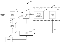
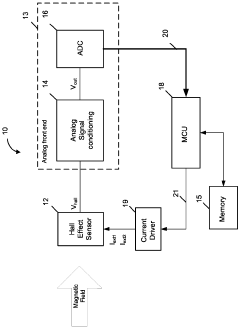
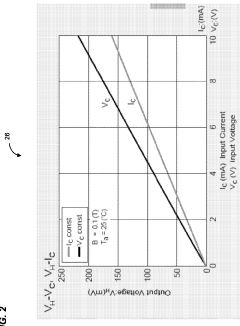
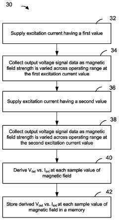
- A method and system that utilize a microcontroller to supply excitation current at different values to the hall effect sensor, obtain corresponding voltage measurements, and verify the sensor's operation based on calibration data, detecting faults in the analog front end and automatically setting the system to a safe mode if measurements are invalid.
Noise Reduction Strategies for Hall Effect Sensors
Noise reduction represents a critical aspect of signal optimization for Hall effect sensors, as these devices are inherently susceptible to various noise sources that can significantly degrade measurement accuracy. Electromagnetic interference (EMI) constitutes one of the primary noise sources affecting Hall sensors, originating from nearby power lines, switching power supplies, or other electronic equipment. To mitigate EMI effects, proper shielding techniques using materials like mu-metal or aluminum enclosures have proven effective in creating Faraday cages that block external electromagnetic fields.
Signal filtering represents another fundamental approach to noise reduction. Low-pass filters effectively eliminate high-frequency noise components while preserving the desired signal. For applications requiring specific frequency responses, band-pass filters can isolate the signal of interest within a defined frequency range. Digital filtering techniques, including moving average filters and Kalman filters, have demonstrated superior performance in dynamic measurement environments by adaptively processing signals based on statistical models.
Differential sensing configurations substantially improve noise immunity by measuring the difference between two Hall elements rather than absolute values. This approach inherently cancels common-mode noise affecting both elements simultaneously. Modern Hall sensor ICs often incorporate chopper stabilization techniques that modulate the Hall voltage to higher frequencies before amplification, effectively separating the signal from low-frequency noise sources like 1/f noise and temperature drift.
Circuit layout optimization plays a crucial role in noise reduction strategies. Implementing proper grounding schemes prevents ground loops that introduce noise, while careful routing of signal traces minimizes capacitive and inductive coupling. Power supply decoupling capacitors placed close to sensor components filter out power rail noise that would otherwise couple into measurements.
Temperature compensation mechanisms address thermal noise and temperature-dependent drift characteristics inherent to semiconductor-based Hall sensors. These include integrated temperature sensors with feedback loops that adjust gain parameters based on temperature readings, or more sophisticated algorithmic approaches that apply correction factors derived from calibration data across operating temperature ranges.
Advanced signal processing techniques have emerged as powerful tools for extracting clean signals from noisy environments. Oversampling combined with decimation increases effective resolution while averaging out random noise components. Adaptive filtering algorithms can dynamically adjust filter parameters based on changing noise characteristics, particularly valuable in applications with variable environmental conditions.
Integration Challenges with IoT and Automotive Applications
The integration of Hall Effect sensors into IoT and automotive applications presents significant technical challenges that require innovative approaches. As these sensors become increasingly vital components in connected devices and modern vehicles, their signal optimization must address the unique demands of these environments. IoT deployments typically require low power consumption, miniaturization, and wireless connectivity, while automotive applications demand extreme reliability, temperature stability, and electromagnetic compatibility.
Power management represents a primary challenge, as IoT devices often operate on limited battery resources or energy harvesting systems. Hall Effect sensors must maintain sensitivity while consuming minimal power, necessitating advanced power gating techniques and intelligent sleep modes. The development of ultra-low-power amplification circuits specifically designed for Hall sensor signals has become a critical research area, with recent innovations achieving sub-microamp current consumption during standby operations.
Miniaturization requirements further complicate integration efforts. As IoT devices and automotive components decrease in size, Hall Effect sensors must maintain performance despite reduced sensing areas and increased proximity to other electronic components. This spatial constraint often leads to signal interference issues, requiring sophisticated shielding techniques and sensor array configurations to maintain signal integrity in compact deployments.
Environmental resilience presents another significant challenge, particularly in automotive applications where sensors must function reliably across extreme temperature ranges (-40°C to 150°C) and withstand vibration, humidity, and electromagnetic interference. Signal optimization techniques must incorporate temperature compensation algorithms and robust filtering to ensure consistent measurements under these variable conditions. Adaptive gain control mechanisms have emerged as a promising solution, automatically adjusting sensitivity parameters based on environmental conditions.
Communication protocol compatibility adds another layer of complexity. Hall Effect sensor signals must be effectively translated into standardized protocols such as CAN bus for automotive applications or low-power wireless protocols like BLE, Zigbee, or LoRaWAN for IoT implementations. This translation process introduces potential latency and signal degradation issues that must be addressed through optimized signal processing chains and efficient data conversion techniques.
Real-time processing requirements further strain integration efforts, particularly in safety-critical automotive systems where sensor data must be processed with minimal latency. Edge computing approaches are increasingly being implemented to process Hall sensor signals locally before transmission, reducing bandwidth requirements and improving response times. However, these approaches must balance processing capabilities with power constraints, particularly in IoT deployments.
Unlock deeper insights with PatSnap Eureka Quick Research — get a full tech report to explore trends and direct your research. Try now!
Generate Your Research Report Instantly with AI Agent
Supercharge your innovation with PatSnap Eureka AI Agent Platform!