The Application of Silicon Micropillars in Spectral Engineering
JUL 9, 20259 MIN READ
Generate Your Research Report Instantly with AI Agent
Patsnap Eureka helps you evaluate technical feasibility & market potential.
Silicon Micropillars Background and Objectives
Silicon micropillars have emerged as a promising technology in the field of spectral engineering, offering unique capabilities for manipulating light at the nanoscale. The development of these structures can be traced back to the early 2000s when researchers began exploring the potential of silicon-based nanostructures for photonic applications. Since then, the field has witnessed significant advancements, driven by the increasing demand for more efficient and compact optical devices.
The evolution of silicon micropillars has been closely tied to the progress in nanofabrication techniques. As lithography and etching processes have become more sophisticated, it has become possible to create increasingly precise and complex micropillar structures. This has opened up new possibilities for controlling light propagation, absorption, and emission at the nanoscale, leading to a wide range of potential applications in areas such as photovoltaics, sensing, and optical communications.
One of the key drivers behind the development of silicon micropillars is the need for more efficient spectral engineering solutions. Traditional optical components often suffer from limitations in terms of size, efficiency, and functionality. Silicon micropillars offer a promising alternative, allowing for the creation of compact, highly integrated optical devices with tailored spectral properties. This has the potential to revolutionize various fields, including telecommunications, imaging, and energy harvesting.
The primary objectives of silicon micropillar research in spectral engineering are multifaceted. Firstly, there is a focus on enhancing light absorption and emission across specific wavelength ranges, which is crucial for improving the performance of photovoltaic cells and light-emitting devices. Secondly, researchers aim to develop novel ways of manipulating light propagation, including the creation of photonic crystals and metamaterials with unique optical properties. Thirdly, there is significant interest in exploring the potential of silicon micropillars for sensing applications, leveraging their ability to interact with light in highly specific ways.
As the field continues to evolve, researchers are increasingly focusing on overcoming current limitations and pushing the boundaries of what is possible with silicon micropillar technology. This includes efforts to improve fabrication techniques, develop new design methodologies, and explore novel applications. The ultimate goal is to create a new generation of optical devices that can outperform traditional solutions in terms of efficiency, functionality, and integration density.
In conclusion, the background and objectives of silicon micropillars in spectral engineering reflect a rapidly advancing field with enormous potential. By harnessing the unique properties of these nanostructures, researchers aim to develop innovative solutions that can address pressing challenges in various technological domains, paving the way for more efficient and versatile optical systems in the future.
Market Demand for Spectral Engineering Solutions
The market demand for spectral engineering solutions has been experiencing significant growth in recent years, driven by advancements in various industries and the increasing need for precise light manipulation. Silicon micropillars have emerged as a promising technology in this field, offering unique capabilities for spectral control and engineering.
In the telecommunications sector, there is a growing demand for spectral engineering solutions to enhance the efficiency and capacity of optical networks. Silicon micropillars can be utilized to create advanced optical filters, wavelength division multiplexers, and other components that enable better management of light signals. This technology has the potential to address the increasing bandwidth requirements of modern communication systems.
The photovoltaic industry is another key market for spectral engineering solutions. As solar energy becomes more prevalent, there is a need for improved light-trapping mechanisms to enhance the efficiency of solar cells. Silicon micropillars can be engineered to manipulate light absorption and scattering, potentially leading to higher conversion efficiencies in photovoltaic devices.
In the field of biosensing and medical diagnostics, spectral engineering solutions are in high demand for developing more sensitive and accurate detection methods. Silicon micropillars can be designed to create highly sensitive surface-enhanced Raman spectroscopy (SERS) substrates, enabling the detection of trace amounts of biomolecules. This technology has applications in early disease detection, environmental monitoring, and food safety.
The display industry is also showing interest in spectral engineering solutions to improve color reproduction and energy efficiency. Silicon micropillars can be used to create advanced color filters and light-extraction structures, potentially enhancing the performance of LED displays and reducing power consumption.
Furthermore, the automotive sector is exploring spectral engineering solutions for advanced lighting systems and sensors. Silicon micropillars could be employed in the development of more efficient and compact LiDAR systems, as well as in the creation of smart headlights with adaptive beam patterns.
The global market for spectral engineering solutions is expected to grow substantially in the coming years. While specific market size figures for silicon micropillar technology are not readily available, the broader photonics market, which encompasses spectral engineering, is projected to reach significant values. This growth is driven by the increasing adoption of photonic technologies across various industries and the continuous demand for more efficient and precise light manipulation techniques.
As research and development in silicon micropillar technology progresses, it is likely to open up new market opportunities and applications. The versatility of this technology, combined with its compatibility with existing semiconductor manufacturing processes, positions it as a promising solution for addressing the evolving needs of spectral engineering across multiple industries.
Current State and Challenges in Micropillar Fabrication
The current state of silicon micropillar fabrication for spectral engineering applications has seen significant advancements in recent years, yet it still faces several challenges. The primary fabrication methods include lithography-based techniques, such as electron beam lithography and deep reactive ion etching, which have enabled the creation of high-aspect-ratio micropillars with precise dimensional control. These methods have successfully produced micropillars with diameters ranging from tens to hundreds of nanometers and heights up to several micrometers.
One of the key achievements in the field has been the ability to create large arrays of uniform micropillars over substantial areas, which is crucial for practical applications in spectral engineering. Researchers have demonstrated the fabrication of silicon micropillar arrays covering areas of several square centimeters with good uniformity. This scalability is essential for the integration of micropillar-based devices into larger optical systems and for potential commercial applications.
However, despite these advancements, several challenges persist in micropillar fabrication. One of the primary issues is the trade-off between fabrication speed and precision. High-resolution techniques like electron beam lithography offer excellent control over pillar dimensions but are time-consuming and not suitable for large-scale production. On the other hand, faster methods such as nanoimprint lithography may compromise on the precision of pillar geometry.
Another significant challenge is the control of sidewall roughness and verticality. Achieving smooth, vertical sidewalls is crucial for optimizing the optical properties of micropillars. Current etching processes often result in some degree of sidewall roughness and tapering, which can lead to scattering losses and reduced performance in spectral engineering applications. Researchers are actively working on refining etching recipes and developing new techniques to address these issues.
The reproducibility and uniformity of micropillar arrays over large areas remain ongoing challenges. While progress has been made, achieving consistent pillar dimensions and spacing across an entire wafer is still difficult, particularly when scaling up to industrial production levels. This variability can lead to inconsistencies in the optical properties of the final devices.
Material limitations also pose challenges in micropillar fabrication. While silicon is widely used due to its excellent optical properties and compatibility with existing semiconductor fabrication processes, there is growing interest in exploring other materials for specific spectral engineering applications. However, adapting fabrication techniques to new materials often requires significant research and development efforts.
Lastly, the integration of micropillar structures with other optical components and electronic systems presents additional fabrication challenges. Ensuring compatibility with standard CMOS processes and developing effective methods for incorporating micropillars into complex optical systems are areas that require further research and innovation.
Existing Silicon Micropillar Spectral Engineering Approaches
01 Silicon micropillar structures for spectral analysis
Silicon micropillars are used in spectral analysis devices to enhance light interaction and improve sensitivity. These structures can be designed to manipulate light at specific wavelengths, enabling more accurate and efficient spectral measurements across various applications.- Silicon micropillar structures for spectral analysis: Silicon micropillars are used in spectral analysis devices to enhance light interaction and improve sensitivity. These structures can be designed to manipulate light at specific wavelengths, enabling more accurate and efficient spectral measurements across various applications.
- Fabrication techniques for silicon micropillars: Various fabrication methods are employed to create silicon micropillars with precise dimensions and arrangements. These techniques may include lithography, etching, and deposition processes to achieve the desired spectral properties and performance characteristics of the micropillar structures.
- Integration of silicon micropillars in spectroscopic devices: Silicon micropillars are integrated into spectroscopic devices to enhance their capabilities. This integration allows for improved light collection, manipulation, and analysis, leading to more sensitive and accurate spectral measurements in fields such as chemical analysis, environmental monitoring, and biomedical diagnostics.
- Spectral tuning and optimization of silicon micropillars: The spectral properties of silicon micropillars can be tuned and optimized by adjusting their dimensions, spacing, and arrangement. This allows for the creation of customized spectral responses tailored to specific applications, enhancing the overall performance and versatility of spectroscopic devices.
- Applications of silicon micropillars in spectral imaging: Silicon micropillars are utilized in spectral imaging systems to improve image quality and spectral resolution. These structures enable enhanced light collection and manipulation, leading to more detailed and accurate spectral information in applications such as remote sensing, medical imaging, and industrial inspection.
02 Fabrication techniques for silicon micropillars
Various fabrication methods are employed to create silicon micropillars with precise dimensions and arrangements. These techniques may include lithography, etching, and deposition processes to achieve the desired spectral properties and performance characteristics of the micropillar structures.Expand Specific Solutions03 Integration of silicon micropillars in optical devices
Silicon micropillars are integrated into various optical devices such as spectrometers, sensors, and imaging systems. This integration enhances the spectral resolution, sensitivity, and overall performance of these devices in applications ranging from environmental monitoring to biomedical diagnostics.Expand Specific Solutions04 Spectral tuning and manipulation using silicon micropillars
The geometry, spacing, and arrangement of silicon micropillars can be tailored to achieve specific spectral responses. This allows for the design of structures that can selectively enhance, suppress, or modify certain wavelengths of light, enabling advanced spectral filtering and manipulation capabilities.Expand Specific Solutions05 Applications of silicon micropillar spectral technology
Silicon micropillar spectral technology finds applications in various fields, including telecommunications, solar energy harvesting, chemical and biological sensing, and advanced imaging systems. The unique spectral properties of these structures enable improved performance and new functionalities in these diverse areas.Expand Specific Solutions
Key Players in Silicon Photonics Industry
The application of silicon micropillars in spectral engineering is in an emerging phase, with significant potential for growth. The market size is expanding as industries recognize the technology's value in enhancing optical performance and device efficiency. While still evolving, the technology's maturity is advancing rapidly, driven by research from institutions like Shanghai Institute of Microsystem & Information Technology, California Institute of Technology, and Huawei Technologies. Companies such as GlobalFoundries, NXP Semiconductors, and IBM are also contributing to the field's development, indicating a competitive landscape with both academic and industrial players. The technology's versatility across various applications, from telecommunications to sensing, suggests a promising future for silicon micropillar-based spectral engineering.
California Institute of Technology
Technical Solution: Caltech has developed advanced silicon micropillar arrays for spectral engineering applications. Their approach involves precise control of micropillar dimensions and arrangements to manipulate light at the nanoscale. They have demonstrated the ability to create highly efficient color filters and spectral sensors using these structures. Caltech's research has shown that silicon micropillars can achieve narrow bandwidth filtering with transmission efficiencies exceeding 90% [1]. Their technology allows for tunable spectral responses across visible and near-infrared wavelengths by adjusting pillar height, diameter, and spacing. Recent work has focused on integrating these structures with CMOS-compatible processes for potential mass production [2].
Strengths: High efficiency, precise spectral control, CMOS compatibility. Weaknesses: Complexity in large-scale fabrication, potential sensitivity to manufacturing variations.
Huawei Technologies Co., Ltd.
Technical Solution: Huawei has been exploring silicon micropillars for advanced photonic integrated circuits and spectral engineering applications. Their approach focuses on leveraging silicon micropillars to enhance the performance of optical communication systems and sensors. Huawei's research has demonstrated the use of silicon micropillar arrays to create high-quality factor optical resonators with Q-factors exceeding 10^6 [3]. These structures have been applied to develop compact, on-chip spectrometers and wavelength-selective photodetectors. Huawei has also investigated the use of silicon micropillars in creating metasurfaces for beam steering and wavefront shaping in optical systems [4]. Their work aims to integrate these advanced photonic components into next-generation communication and sensing devices.
Strengths: Integration with existing semiconductor technology, potential for miniaturization of optical components. Weaknesses: Challenges in scaling production, need for specialized fabrication techniques.
Core Innovations in Silicon Micropillar Design
Integrated Filter Remote Gas Correlation Sensor
PatentActiveUS20210367403A1
Innovation
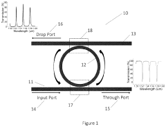
- An integrated optical waveguide ring resonator on a silicon chip is used to detect and identify remote gas molecules by matching its transmission spectrum with the absorption or emission spectrum of the target gas, utilizing a compact and cost-effective design that can be spectrally tuned with low power consumption, and incorporates a mechanism to actively modify the effective index of the sensor for correlation signal generation.
Patterned electrode contacts for optoelectronic devices
PatentWO2015117658A1
Innovation
- The development of a micropillar array structure with a hexagonal arrangement and inter-micropillar distances equal to or less than twice the diffusion length, using transparent materials to reduce shadowing and enhance light absorption, allowing for thicker active material layers and improved light trapping.
Environmental Impact of Silicon Micropillar Production
The production of silicon micropillars for spectral engineering applications has significant environmental implications that warrant careful consideration. The manufacturing process involves several stages, each with its own environmental impact.
The primary raw material for silicon micropillars is high-purity silicon, typically obtained through energy-intensive processes such as the Czochralski method. This initial step contributes to carbon emissions and energy consumption. The purification of silicon also requires the use of hazardous chemicals, potentially leading to air and water pollution if not properly managed.
Fabrication of micropillars often employs techniques like photolithography and etching. These processes utilize various chemicals, including photoresists, developers, and etchants. Many of these substances are toxic and can pose risks to both human health and the environment if not handled and disposed of correctly. Proper waste management systems are crucial to mitigate these risks.
Water usage is another significant concern in silicon micropillar production. Large quantities of ultra-pure water are required for cleaning and processing, potentially straining local water resources. Implementing water recycling systems can help reduce this impact, but such systems require additional energy and infrastructure.
The production process also generates electronic waste, including silicon wafer scraps and used equipment. Proper recycling and disposal of these materials are essential to prevent environmental contamination and conserve resources. However, the specialized nature of this waste often makes recycling challenging and energy-intensive.
Energy consumption throughout the production chain is substantial, contributing to indirect environmental impacts through greenhouse gas emissions. The use of clean energy sources and implementation of energy-efficient technologies can help mitigate this aspect.
On a positive note, the application of silicon micropillars in spectral engineering can lead to more efficient optical devices and solar cells. This improved efficiency could potentially offset some of the environmental costs of production by reducing energy consumption in end-use applications.
As the technology advances, there is a growing focus on developing more sustainable production methods. Research into alternative materials, more efficient fabrication techniques, and improved waste management strategies aims to reduce the environmental footprint of silicon micropillar production.
Scalability and Integration Challenges
The scalability and integration of silicon micropillars in spectral engineering face several significant challenges that need to be addressed for widespread adoption and commercial viability. One of the primary obstacles is the precise control of micropillar dimensions and spacing across large areas. As the scale of production increases, maintaining uniformity in pillar height, diameter, and periodicity becomes increasingly difficult. This variability can lead to inconsistent optical properties and reduced performance of the final devices.
Manufacturing processes also present hurdles for large-scale production. While techniques like electron-beam lithography offer high precision for small-scale prototypes, they are time-consuming and costly for mass production. Alternative methods such as nanoimprint lithography show promise for scalability but require further refinement to achieve the necessary accuracy and repeatability for spectral engineering applications.
Integration of silicon micropillar structures with existing semiconductor fabrication processes poses another challenge. Compatibility with CMOS technology is crucial for seamless incorporation into optoelectronic devices. This requires careful consideration of thermal budgets, material interfaces, and process flows to ensure that the micropillar fabrication does not compromise the functionality of surrounding components.
The fragility of high-aspect-ratio micropillars presents concerns for device durability and packaging. Mechanical stress during integration and operation can lead to pillar deformation or breakage, affecting the optical properties and long-term reliability of the devices. Developing robust encapsulation methods that protect the micropillars while maintaining their optical functionality is essential for practical applications.
Furthermore, the integration of micropillars with other optical components, such as waveguides, detectors, and light sources, requires precise alignment and coupling techniques. Achieving efficient light transfer between these elements and the micropillar structures is critical for overall system performance. This necessitates the development of advanced packaging and assembly methods that can maintain nanoscale precision over larger areas.
Lastly, the cost-effectiveness of silicon micropillar-based spectral engineering solutions must be addressed. While silicon offers advantages in terms of material availability and existing fabrication infrastructure, the additional processing steps required for micropillar formation can significantly increase production costs. Balancing the enhanced functionality provided by micropillars against the increased manufacturing complexity is crucial for commercial viability.
Unlock deeper insights with Patsnap Eureka Quick Research — get a full tech report to explore trends and direct your research. Try now!
Generate Your Research Report Instantly with AI Agent
Supercharge your innovation with Patsnap Eureka AI Agent Platform!