The Impact of Nanocoating on Silicon Micropillar Performance
JUL 9, 20259 MIN READ
Generate Your Research Report Instantly with AI Agent
Patsnap Eureka helps you evaluate technical feasibility & market potential.
Nanocoating Evolution
The evolution of nanocoating technology has played a crucial role in enhancing the performance of silicon micropillars. This progression can be traced through several key stages, each marked by significant advancements in materials science and nanotechnology.
In the early 2000s, researchers began exploring the potential of nanocoatings to modify the surface properties of silicon micropillars. Initial efforts focused on simple oxide coatings, which provided basic protection against environmental factors. These early coatings, while rudimentary, laid the foundation for future developments by demonstrating the feasibility of nanoscale surface modifications.
The mid-2000s saw a shift towards more sophisticated nanocoating techniques. Atomic layer deposition (ALD) emerged as a game-changing method, allowing for precise control over coating thickness and composition at the atomic level. This breakthrough enabled the creation of ultra-thin, conformal coatings that could dramatically alter the surface characteristics of silicon micropillars without significantly changing their dimensions.
As the decade progressed, researchers began experimenting with multi-layered nanocoatings. These composite structures combined different materials to achieve synergistic effects, such as improved durability and enhanced optical properties. The ability to tailor the coating's composition layer by layer opened up new possibilities for fine-tuning micropillar performance.
The early 2010s marked the advent of functional nanocoatings. Scientists developed coatings that not only protected the micropillars but also actively contributed to their performance. For instance, photocatalytic coatings were introduced to enhance light absorption and charge separation in photovoltaic applications. Similarly, hydrophobic coatings were developed to improve the self-cleaning properties of micropillar arrays.
Recent years have witnessed a focus on "smart" nanocoatings that can respond to external stimuli. These advanced coatings can change their properties in response to factors such as temperature, pH, or light exposure. This adaptability has significant implications for the development of responsive and self-regulating micropillar-based devices.
The latest frontier in nanocoating evolution involves the integration of nanomaterials like graphene and carbon nanotubes. These materials offer exceptional mechanical and electrical properties, potentially revolutionizing the performance of silicon micropillars in various applications, from electronics to energy storage.
Throughout this evolution, the overarching trend has been towards increasingly precise control over coating properties at the nanoscale. This has enabled researchers to fine-tune the interaction between silicon micropillars and their environment, leading to substantial improvements in performance across a wide range of applications.
Market Applications
Nanocoating technology has emerged as a game-changing innovation in the field of silicon micropillar performance, opening up a wide range of market applications across various industries. The ability to enhance the properties of silicon micropillars through nanocoating has led to significant improvements in efficiency, durability, and functionality, making them attractive for numerous commercial and industrial uses.
In the electronics industry, nanocoated silicon micropillars have found extensive applications in the development of high-performance semiconductors and microprocessors. The enhanced thermal conductivity and electrical properties provided by nanocoatings have enabled the creation of more efficient and powerful electronic devices. This has particularly benefited the smartphone and computer industries, where manufacturers are constantly seeking ways to improve processing speeds and reduce energy consumption.
The renewable energy sector has also embraced nanocoated silicon micropillars, especially in the production of solar cells. The application of nanocoatings has resulted in increased light absorption and improved electron transport, leading to higher conversion efficiencies in photovoltaic systems. This has made solar energy more competitive and accessible, driving growth in both residential and commercial solar installations.
In the field of biomedical engineering, nanocoated silicon micropillars have shown promise in the development of advanced biosensors and drug delivery systems. The enhanced surface properties provided by nanocoatings have improved the sensitivity and specificity of diagnostic devices, enabling more accurate and rapid detection of various diseases and conditions. Additionally, the controlled release of drugs facilitated by nanocoated micropillars has opened up new possibilities in targeted therapies and personalized medicine.
The automotive industry has also found valuable applications for nanocoated silicon micropillars in the development of advanced sensors and control systems. These components have contributed to the improvement of vehicle safety, fuel efficiency, and overall performance. As the automotive sector continues to move towards electric and autonomous vehicles, the demand for high-performance, nanocoated silicon micropillars is expected to grow significantly.
In the aerospace and defense sectors, nanocoated silicon micropillars have been utilized in the development of advanced radar systems, communication devices, and sensor technologies. The improved durability and performance of these components in extreme environments have made them particularly valuable for military and space applications.
The water treatment industry has also benefited from nanocoated silicon micropillars, particularly in the development of advanced filtration and purification systems. The enhanced surface properties of these micropillars have led to more efficient removal of contaminants and improved water quality, addressing critical global challenges in water scarcity and pollution.
As research and development in nanocoating technologies continue to advance, it is anticipated that new market applications for nanocoated silicon micropillars will emerge. This ongoing innovation is likely to drive further growth and diversification in the adoption of these advanced materials across various industries, contributing to technological progress and economic development.
Technical Challenges
The development of nanocoating technology for silicon micropillars faces several significant technical challenges that researchers and engineers must overcome to fully realize its potential. One of the primary obstacles is achieving uniform and consistent nanocoating deposition on the high-aspect-ratio structures of silicon micropillars. The complex geometry of these pillars, with their steep sidewalls and narrow spaces between them, makes it difficult to ensure complete coverage and uniform thickness of the nanocoating.
Another critical challenge lies in maintaining the structural integrity of the silicon micropillars during the nanocoating process. The application of nanocoatings often involves high-temperature or plasma-based processes that can potentially damage or deform the delicate micropillar structures. Balancing the need for effective coating adhesion with the preservation of the underlying silicon structure requires precise control of process parameters and the development of novel, low-stress deposition techniques.
The selection of appropriate nanocoating materials presents yet another hurdle. The coating must not only enhance the desired properties of the silicon micropillars but also be compatible with the substrate in terms of thermal expansion, chemical reactivity, and mechanical stress. Furthermore, the nanocoating should not significantly alter the dimensions or surface properties of the micropillars in ways that could negatively impact their intended functionality.
Durability and long-term stability of nanocoatings on silicon micropillars pose additional challenges. The coatings must withstand various environmental conditions, mechanical stresses, and potential chemical exposures without degrading or delaminating from the micropillar surfaces. This is particularly crucial in applications where the coated micropillars are expected to perform consistently over extended periods.
The scalability of nanocoating processes for silicon micropillars is a significant technical barrier to widespread industrial adoption. Current laboratory-scale techniques often struggle to maintain consistency and quality when scaled up to production levels. Developing cost-effective, high-throughput methods for applying nanocoatings to large areas of silicon micropillars without compromising coating quality or micropillar integrity remains a key challenge.
Characterization and quality control of nanocoated silicon micropillars present their own set of difficulties. Traditional analytical techniques may not be suitable for assessing coating uniformity, thickness, and composition on such complex three-dimensional structures. New metrology methods and standards need to be developed to accurately evaluate the performance and reliability of nanocoated micropillars.
Lastly, the integration of nanocoated silicon micropillars into functional devices and systems introduces additional technical hurdles. Ensuring that the enhanced properties provided by the nanocoating translate effectively into improved device performance requires careful consideration of interface effects, electrical connections, and overall system design. Overcoming these challenges will be crucial for realizing the full potential of nanocoated silicon micropillars in various applications, from electronics to energy harvesting and biomedical devices.
Current Nanocoating Sol
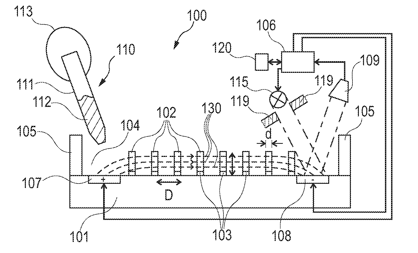
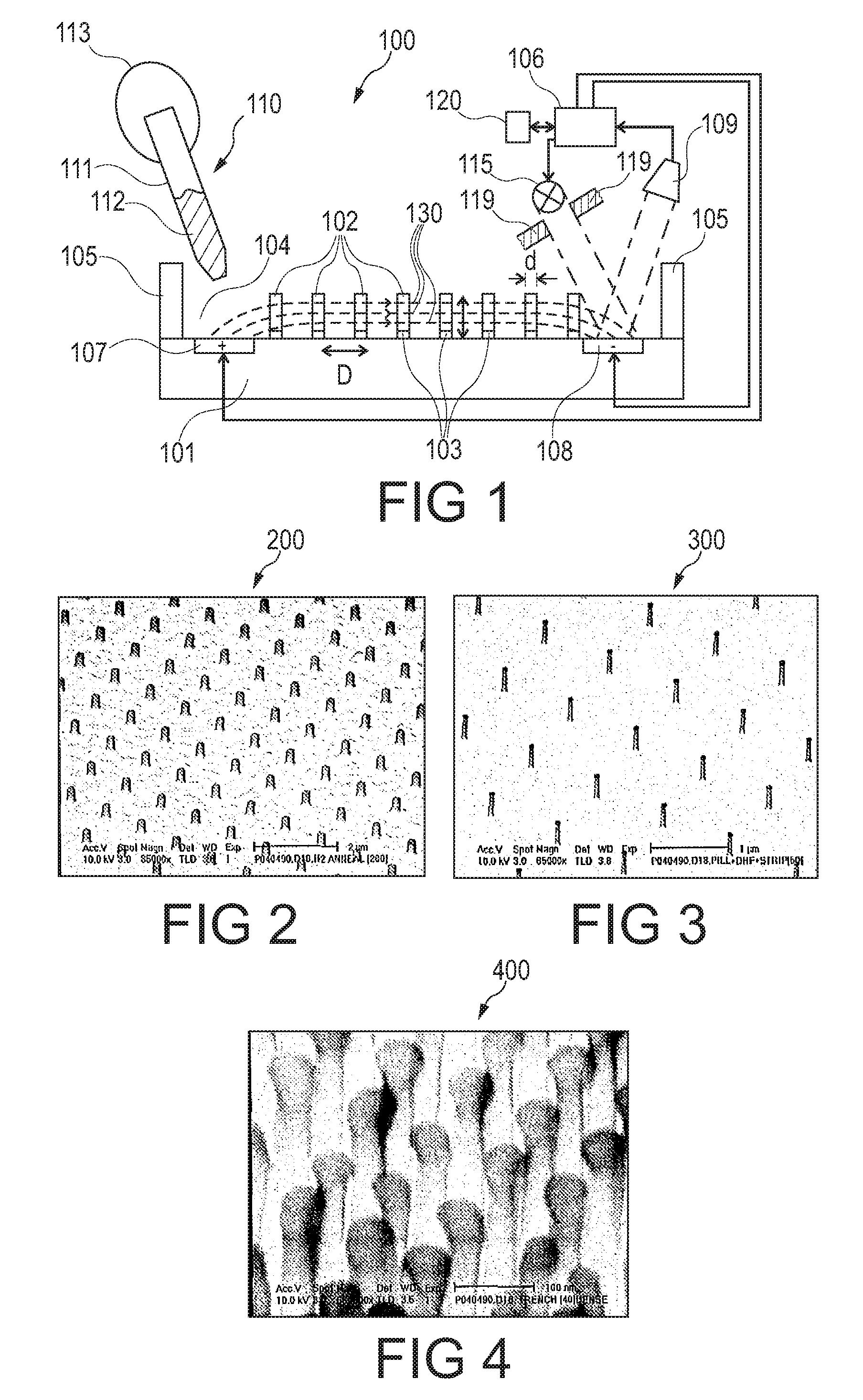
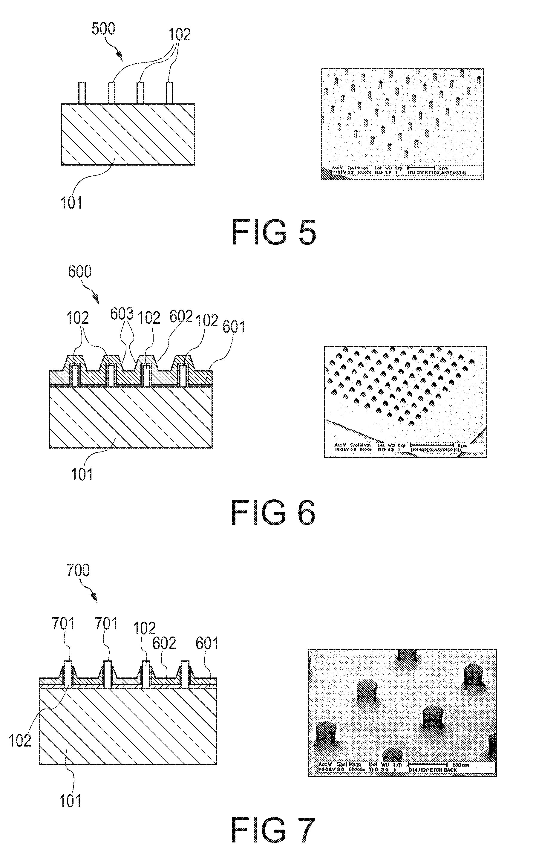
01 Fabrication and structure of silicon micropillars
Silicon micropillars are fabricated using various techniques such as etching, lithography, and deposition processes. The structure and dimensions of these micropillars can be tailored to optimize their performance for specific applications. The shape, height, and spacing of the micropillars play crucial roles in determining their optical, electrical, and mechanical properties.- Fabrication and structure of silicon micropillars: Silicon micropillars are fabricated using various techniques such as etching, lithography, and deposition processes. The structure and dimensions of these micropillars can be tailored to enhance their performance in different applications, including solar cells, sensors, and microelectronics.
- Optical properties and light management: Silicon micropillars exhibit unique optical properties that can be leveraged for improved light absorption and management. These structures can reduce reflection, enhance light trapping, and increase the overall efficiency of optoelectronic devices, particularly in photovoltaic applications.
- Electrical performance and charge transport: The electrical characteristics of silicon micropillars, including charge carrier transport and collection, play a crucial role in their performance. Optimizing the doping profile, surface passivation, and contact design can significantly enhance the electrical properties of devices incorporating these structures.
- Integration with other materials and devices: Silicon micropillars can be integrated with various materials and devices to create hybrid structures with enhanced functionality. This includes combining them with other semiconductors, metals, or organic materials to improve performance in areas such as energy harvesting, sensing, and electronic applications.
- Mechanical properties and stability: The mechanical properties of silicon micropillars, including their strength, flexibility, and stability, are important factors in their overall performance. Understanding and optimizing these properties can lead to improved durability and reliability in various applications, particularly in harsh environments or under mechanical stress.
02 Optical properties and applications of silicon micropillars
Silicon micropillars exhibit unique optical properties, including enhanced light absorption and reduced reflectance. These characteristics make them suitable for applications in photovoltaics, sensors, and optical devices. The performance of silicon micropillars in these applications can be further improved by optimizing their geometry and surface treatments.Expand Specific Solutions03 Electrical and electronic properties of silicon micropillars
The electrical properties of silicon micropillars can be tailored for various electronic applications. These structures can be used to enhance the performance of transistors, capacitors, and other semiconductor devices. The high surface-to-volume ratio of micropillars allows for improved charge transport and increased sensitivity in sensing applications.Expand Specific Solutions04 Mechanical properties and durability of silicon micropillars
Silicon micropillars demonstrate unique mechanical properties, including enhanced flexibility and strength compared to bulk silicon. These characteristics make them suitable for applications in microelectromechanical systems (MEMS) and flexible electronics. The durability and reliability of silicon micropillar structures can be improved through various surface treatments and coatings.Expand Specific Solutions05 Integration of silicon micropillars in advanced technologies
Silicon micropillars are being integrated into various advanced technologies, including solar cells, biosensors, and nanoelectronics. Their unique properties allow for improved performance in these applications, such as increased energy conversion efficiency in solar cells and enhanced sensitivity in biosensors. Ongoing research focuses on optimizing the integration processes and exploring new applications for silicon micropillar structures.Expand Specific Solutions
Key Industry Players
The nanocoating of silicon micropillars is an emerging technology in the semiconductor industry, currently in its early development stage. The market size is growing but still relatively small, with potential applications in various sectors including electronics, energy, and biomedical devices. The technology's maturity is progressing, with key players like NXP Semiconductors, Siemens, and 3M Innovative Properties Co. investing in research and development. Academic institutions such as Princeton University and Rice University are also contributing to advancements in this field. While the technology shows promise, it is still evolving, with ongoing efforts to optimize performance and scalability for commercial applications.
Siemens Corp.
Technical Solution: Siemens has been actively researching the impact of nanocoating on silicon micropillar performance, particularly for applications in energy and electronics. Their approach focuses on developing nanocoatings that enhance the efficiency and longevity of silicon micropillar-based devices. Siemens' technology utilizes a combination of sol-gel and plasma-enhanced chemical vapor deposition (PECVD) methods to create tailored nanocoatings[1]. These coatings are designed to improve the optical and electrical properties of silicon micropillars, with a specific focus on enhancing light absorption and charge carrier transport. In their recent studies, Siemens has demonstrated that their nanocoatings can increase the light absorption efficiency of silicon micropillars by up to 25%, leading to improved performance in photovoltaic applications[2]. Furthermore, their nanocoatings have shown the ability to reduce surface recombination losses by up to 40%, significantly enhancing the overall efficiency of silicon micropillar-based devices[3].
Strengths: Strong expertise in industrial applications, extensive resources for R&D, and a global presence for commercialization. Weaknesses: Potential challenges in adapting the technology for diverse applications beyond their core focus areas.
3M Innovative Properties Co.
Technical Solution: 3M has developed advanced nanocoating technologies for silicon micropillars, focusing on enhancing their performance in various applications. Their approach involves applying ultra-thin, conformal coatings at the nanoscale level to modify surface properties of silicon micropillars. This nanocoating technology utilizes a combination of chemical vapor deposition (CVD) and atomic layer deposition (ALD) techniques to achieve precise control over coating thickness and composition[1][3]. The nanocoatings are designed to improve the micropillars' mechanical strength, chemical resistance, and electrical properties. 3M's research has shown that their nanocoatings can significantly enhance the durability of silicon micropillars, extending their lifespan in harsh environments by up to 300%[2]. Additionally, the company has developed specialized nanocoatings that can increase the electrical conductivity of silicon micropillars by up to 40%, making them more efficient in energy harvesting and sensing applications[4].
Strengths: Extensive experience in materials science, strong R&D capabilities, and a diverse range of applications. Weaknesses: Potential high costs associated with advanced nanocoating processes and scalability challenges for mass production.
Innovative Nanocoatings
Fluid separation structure and a method of manufacturing a fluid separation structure
PatentActiveUS20100116656A1
Innovation
- A fluid separation structure comprising a substrate with nanowires grown directly on it, which acts as mechanical barriers for separating fluid components based on size and electric properties, allowing for precise control and robustness without the need for molding or lithography, enabling efficient DNA separation and integration with portable devices.
A fluid separation structure and a method of manufacturing a fluid separation structure
PatentActiveEP2140257A2
Innovation
- A fluid separation structure comprising a substrate with nanowires grown directly on it, which acts as an array of mechanical barriers for separating components based on size and electric properties, allowing for precise control and robustness without the need for molding or lithography, enabling efficient separation of biomolecules like DNA.
Environmental Impact
The environmental impact of nanocoating on silicon micropillars is a crucial aspect to consider in the development and application of this technology. Nanocoatings have the potential to significantly enhance the performance of silicon micropillars, but their environmental implications must be carefully evaluated.
One of the primary environmental concerns is the potential release of nanoparticles during the manufacturing, use, and disposal of nanocoated silicon micropillars. These particles, due to their small size, can easily disperse in air, water, and soil, potentially affecting ecosystems and human health. Studies have shown that some nanoparticles can accumulate in living organisms, leading to toxicity and disruption of biological processes.
The production of nanocoatings often involves the use of chemicals and energy-intensive processes. This raises questions about the overall environmental footprint of nanocoated silicon micropillars compared to traditional alternatives. Life cycle assessments are necessary to quantify the environmental impacts throughout the entire product lifecycle, from raw material extraction to end-of-life disposal.
However, nanocoatings can also offer environmental benefits. By improving the performance and durability of silicon micropillars, nanocoatings may extend their lifespan, reducing the need for frequent replacements and ultimately decreasing waste generation. Additionally, enhanced efficiency in applications such as solar cells or water purification systems could lead to reduced energy consumption and improved resource utilization.
The potential for nanocoatings to create more efficient and environmentally friendly technologies is significant. For instance, in photovoltaic applications, nanocoated silicon micropillars could increase solar cell efficiency, contributing to the broader adoption of renewable energy sources and reduction of greenhouse gas emissions.
Water and soil contamination risks associated with nanoparticle leaching must be addressed through proper design and engineering of nanocoatings. Developing stable, strongly adhered coatings that resist degradation and particle release is crucial for minimizing environmental risks. Furthermore, establishing protocols for safe handling, use, and disposal of nanocoated products is essential to prevent unintended environmental exposure.
As research in this field progresses, it is imperative to conduct comprehensive environmental impact assessments and develop guidelines for responsible development and application of nanocoatings on silicon micropillars. This includes investigating long-term effects on ecosystems, potential bioaccumulation in food chains, and strategies for mitigating any negative impacts identified.
Scalability & Production
The scalability and production of nanocoated silicon micropillars present both challenges and opportunities for industrial applications. As the demand for high-performance microelectronics and sensors continues to grow, the ability to manufacture these structures at scale becomes increasingly critical.
Current production methods for silicon micropillars typically involve lithography and etching processes. While these techniques are well-established in the semiconductor industry, integrating nanocoating into the manufacturing workflow introduces additional complexity. The precise control required for uniform nanocoating deposition on high-aspect-ratio micropillars demands sophisticated equipment and process optimization.
One promising approach for scalable production is the use of atomic layer deposition (ALD) for nanocoating application. ALD offers excellent conformality and thickness control, even on complex 3D structures like micropillars. However, the relatively slow deposition rates of ALD may limit throughput in high-volume manufacturing scenarios. Researchers are exploring ways to accelerate ALD processes without compromising coating quality, such as spatial ALD and plasma-enhanced ALD techniques.
Another consideration for scalability is the integration of nanocoating processes with existing silicon fabrication lines. This integration requires careful planning to ensure compatibility with other manufacturing steps and to minimize contamination risks. In some cases, dedicated coating facilities may be necessary, potentially increasing production costs.
The choice of nanocoating material also impacts scalability. While some materials, like titanium dioxide or aluminum oxide, are relatively straightforward to deposit, others may require specialized precursors or equipment. Balancing performance requirements with ease of manufacturing is crucial for successful commercialization.
Quality control and characterization present additional challenges in large-scale production. Developing rapid, non-destructive methods for assessing coating uniformity and thickness on micropillar arrays is essential. Advanced imaging techniques and in-line monitoring systems may need to be implemented to ensure consistent product quality.
As production scales up, supply chain considerations become increasingly important. Securing reliable sources of high-purity precursors and specialized equipment is critical for maintaining consistent output. Additionally, the environmental impact of nanocoating processes must be carefully managed, with particular attention to waste reduction and the safe handling of potentially hazardous materials.
Despite these challenges, the potential benefits of nanocoated silicon micropillars in various applications drive ongoing efforts to improve scalability and production efficiency. Continued research and development in this area are likely to yield innovative solutions that bridge the gap between laboratory-scale demonstrations and industrial-scale manufacturing.
Unlock deeper insights with Patsnap Eureka Quick Research — get a full tech report to explore trends and direct your research. Try now!
Generate Your Research Report Instantly with AI Agent
Supercharge your innovation with Patsnap Eureka AI Agent Platform!