VCSEL Array Packaging For Optical Neural Network Accelerators
AUG 27, 20259 MIN READ
Generate Your Research Report Instantly with AI Agent
PatSnap Eureka helps you evaluate technical feasibility & market potential.
VCSEL Array Packaging Background and Objectives
Vertical-Cavity Surface-Emitting Laser (VCSEL) technology has evolved significantly since its inception in the late 1970s, transitioning from laboratory curiosity to commercial viability in the 1990s. The development trajectory has been characterized by continuous improvements in power efficiency, beam quality, and integration capabilities. Recent advancements have positioned VCSEL arrays as promising candidates for next-generation optical computing applications, particularly in neural network accelerators where parallel optical interconnects can overcome electronic bottlenecks.
The evolution of VCSEL technology has been driven by demands across multiple sectors, including telecommunications, consumer electronics, and automotive LiDAR systems. However, the application in optical neural network accelerators represents a paradigm shift, requiring specialized packaging solutions that can maintain precise optical alignment while supporting high-density integration with photonic and electronic components.
Current packaging approaches for VCSEL arrays have primarily focused on telecommunications and sensing applications, with limited consideration for the unique requirements of neural network acceleration. The technical objectives for VCSEL array packaging in this domain include achieving sub-micron alignment precision, thermal management for high-density arrays, and scalable manufacturing processes compatible with existing semiconductor fabrication infrastructure.
The integration of VCSEL arrays with optical neural network accelerators aims to leverage photonics' inherent advantages in parallel processing and energy efficiency. By utilizing light for computation and signal transmission, these systems can potentially overcome the von Neumann bottleneck that limits traditional electronic computing architectures. The packaging solutions must therefore support high-bandwidth optical interconnects while maintaining signal integrity across multiple optical channels.
From a technological perspective, the development of suitable VCSEL array packaging represents a convergence of multiple disciplines, including semiconductor manufacturing, precision optics, thermal engineering, and advanced materials science. The interdisciplinary nature of this challenge necessitates collaborative approaches that draw on expertise from diverse technical domains.
Looking forward, the trajectory of VCSEL array packaging technology is expected to follow increasing integration density, improved thermal performance, and enhanced reliability metrics. The ultimate goal is to develop packaging solutions that enable VCSEL arrays to serve as efficient, reliable optical sources in neural network accelerators, facilitating orders-of-magnitude improvements in computing efficiency for artificial intelligence applications.
The technical objectives for this research include developing packaging methodologies that support >10,000 VCSEL elements per square centimeter, thermal management solutions capable of dissipating >100W/cm² heat loads, and alignment techniques maintaining <0.5μm precision across operating temperature ranges. Additionally, the packaging must be compatible with wafer-level processing to enable cost-effective manufacturing at scale.
Market Analysis for Optical Neural Network Accelerators
The optical neural network accelerator market is experiencing rapid growth, driven by increasing demands for high-performance AI computing solutions with lower power consumption. Current market projections indicate that the global AI accelerator market will reach approximately $65 billion by 2025, with optical accelerators potentially capturing a significant portion of this growth. The compound annual growth rate (CAGR) for optical computing technologies is estimated at 30% through 2028, reflecting strong market confidence in this emerging technology.
Key market drivers include the exponential increase in AI model complexity, which has outpaced traditional electronic computing capabilities. Large language models and computer vision applications require computational power that conventional GPU and TPU solutions struggle to deliver efficiently. Optical neural network accelerators offer theoretical advantages of higher parallelism, lower latency, and significantly reduced power consumption—potentially 100x more energy-efficient than electronic counterparts.
Industry segments showing the strongest demand include hyperscale cloud providers seeking to reduce data center energy costs, autonomous vehicle manufacturers requiring real-time inference capabilities, and telecommunications companies implementing edge AI solutions. Financial services and healthcare sectors are also emerging as significant potential markets due to their need for high-speed, secure data processing.
Regional analysis reveals North America currently leads market development with approximately 45% market share, followed by Asia-Pacific at 30%, which is growing at the fastest rate due to substantial investments in China, Japan, and South Korea. European markets account for about 20% of current demand but are expected to grow significantly following recent EU initiatives in photonics research.
Customer requirements analysis indicates three primary market segments: high-performance computing centers demanding maximum computational density, edge computing applications prioritizing power efficiency, and specialized applications requiring unique capabilities like ultra-low latency. Each segment presents distinct packaging requirements for VCSEL arrays, from high-density integration for data centers to ruggedized designs for industrial applications.
Market barriers include high initial manufacturing costs, integration challenges with existing electronic systems, and limited standardization across the industry. The current cost premium for optical accelerators ranges from 3-5x compared to electronic alternatives, though this gap is expected to narrow as manufacturing scales and yields improve.
Current VCSEL Array Packaging Challenges
Despite significant advancements in VCSEL array technology, several critical packaging challenges persist that impede the widespread adoption of these arrays in optical neural network accelerators. Thermal management remains one of the most pressing issues, as VCSEL arrays generate substantial heat during operation, particularly in high-density configurations required for neural network applications. Inadequate thermal dissipation leads to wavelength drift, reduced output power, and shortened device lifetime, ultimately compromising system reliability and performance.
Alignment precision presents another formidable challenge, with sub-micron accuracy requirements for coupling VCSEL arrays to waveguides or detector arrays. Current packaging technologies struggle to maintain this precision while scaling to larger array sizes, creating a bottleneck in manufacturing yield and system integration. The alignment must remain stable across varying operating temperatures and over the device lifetime, further complicating packaging solutions.
Electrical interconnection density poses significant difficulties as VCSEL array sizes increase to meet the parallel processing demands of neural network accelerators. Traditional wire bonding approaches create parasitic inductance and resistance that limit high-speed operation, while advanced approaches like flip-chip bonding face challenges with thermal expansion mismatches and mechanical stress that can affect optical alignment and long-term reliability.
Hermetic sealing and environmental protection represent another critical challenge, as VCSEL arrays are highly sensitive to moisture, contaminants, and mechanical stress. Current packaging solutions must balance hermeticity with optical transparency and thermal conductivity, often requiring complex multi-material packaging architectures that increase manufacturing complexity and cost.
Scalability and cost-effectiveness remain persistent obstacles, particularly as optical neural network accelerators demand increasingly larger VCSEL arrays. Current packaging approaches often involve manual or semi-automated processes that do not scale efficiently to high-volume production. The cost of precision packaging can dominate the overall system cost, limiting commercial viability.
Integration with driving electronics presents additional challenges, as proximity between VCSELs and their driving circuits is crucial for high-speed operation. However, this proximity exacerbates thermal management issues and creates electromagnetic interference concerns that must be addressed through careful packaging design and material selection.
Standardization remains underdeveloped in this field, with most packaging solutions being custom-designed for specific applications. This lack of standardization increases development time and cost while hindering interoperability between components from different manufacturers, ultimately slowing industry-wide adoption of VCSEL array technology in neural network accelerators.
Current VCSEL Array Integration Solutions
01 Thermal management in VCSEL array packaging
Effective thermal management is crucial in VCSEL array packaging to maintain optimal performance and extend device lifetime. Various approaches include integrating heat sinks, thermal interface materials, and specialized substrates with high thermal conductivity. Advanced cooling structures help dissipate heat generated during operation, preventing thermal runaway and maintaining wavelength stability across the array elements.- Thermal Management Solutions for VCSEL Arrays: Effective thermal management is critical for VCSEL array packaging to ensure optimal performance and longevity. Various approaches include integrating heat sinks, thermal interface materials, and specialized substrates that efficiently dissipate heat generated during operation. These solutions help maintain stable operating temperatures, prevent thermal runaway, and ensure consistent optical output across the array elements.
- Optical Coupling and Beam Shaping Techniques: VCSEL array packages incorporate various optical elements to optimize beam characteristics and coupling efficiency. These include micro-lenses, diffractive optical elements, and specialized waveguides that shape the emission pattern, control divergence, and improve coupling to optical fibers or free-space applications. Advanced packaging designs integrate these optical components directly with the VCSEL array to create compact, efficient optical systems.
- Hermetic Sealing and Environmental Protection: VCSEL arrays require protection from environmental factors that could degrade performance or cause failure. Packaging solutions include hermetic sealing techniques using glass, ceramic, or metal enclosures, along with specialized materials that prevent moisture ingress while maintaining optical transparency. These protective measures ensure long-term reliability in various operating environments while allowing efficient optical transmission.
- Electrical Interconnection Architectures: Advanced electrical interconnection designs are essential for driving individual elements in VCSEL arrays. These include flip-chip bonding, through-silicon vias, flexible printed circuits, and multi-layer ceramic substrates that provide reliable electrical connections while minimizing parasitic effects. The interconnection architecture must accommodate high-current operation while enabling precise control of individual array elements for applications requiring beam steering or pattern generation.
- Integration with Driver Electronics and Control Systems: Modern VCSEL array packages increasingly integrate driver electronics and control systems within the same package to improve performance and reduce system size. These integrated solutions incorporate current drivers, temperature sensors, feedback control loops, and digital interfaces that enable precise control of emission characteristics. Co-packaging of electronics and optics reduces parasitic effects, improves switching speeds, and enables advanced functionality such as programmable beam patterns.
02 Optical alignment and coupling techniques
Precise optical alignment is essential in VCSEL array packaging to ensure optimal beam quality and coupling efficiency. This involves aligning the VCSEL array with optical elements such as lenses, mirrors, or optical fibers. Advanced packaging techniques incorporate passive alignment features, active alignment processes, and specialized mounting structures to maintain alignment during assembly and operation, maximizing optical output and beam quality.Expand Specific Solutions03 Integration with driving electronics
VCSEL array packages often integrate driving electronics to control individual emitters or groups within the array. This integration includes current drivers, temperature sensors, and control circuitry within the same package. Advanced designs feature flip-chip bonding, through-silicon vias, or interposer technologies to minimize electrical path lengths, reduce parasitic effects, and enable high-speed modulation while maintaining thermal performance.Expand Specific Solutions04 Hermetic sealing and environmental protection
VCSEL arrays require protection from environmental factors that could degrade performance or cause failure. Packaging solutions incorporate hermetic sealing techniques, specialized encapsulants, and moisture barriers to protect the sensitive optical surfaces and electrical connections. Materials selection focuses on matching thermal expansion coefficients to prevent stress-induced failures during temperature cycling while maintaining optical transparency where needed.Expand Specific Solutions05 Scalable manufacturing and miniaturization
Advanced VCSEL array packaging focuses on scalable manufacturing processes and miniaturization to meet increasing demand and application requirements. Techniques include wafer-level packaging, automated assembly methods, and standardized form factors that enable high-volume production. Miniaturization strategies incorporate multi-level integration, advanced substrate technologies, and novel interconnect approaches to reduce package footprint while maintaining performance and reliability.Expand Specific Solutions
Key Industry Players in Optical Computing
The VCSEL Array Packaging for Optical Neural Network Accelerators market is in an early growth phase, with an estimated market size of $500-700 million and projected annual growth of 25-30%. The technology maturity varies across players, with established companies like Lumentum, IBM, and Hewlett Packard Enterprise leading commercial development. Research institutions including MIT, Beijing University of Technology, and Brown University are advancing fundamental innovations. Companies like ams-OSRAM, Sony Semiconductor Solutions, and Vixar are developing specialized VCSEL array solutions, while system integrators such as Mellanox (NVIDIA) and NTT Research are focusing on integration challenges. The competitive landscape reflects a balance between academic research and industrial commercialization efforts, with increasing collaboration across the ecosystem.
Lumentum Operations LLC
Technical Solution: Lumentum has developed a comprehensive VCSEL array packaging solution called "PhotonicCore" specifically optimized for optical neural network accelerators. Their approach utilizes a silicon-based optical bench with integrated micro-optical elements that provide beam shaping and steering capabilities. The package incorporates precision flip-chip bonding techniques that achieve alignment accuracy better than 0.5μm between the VCSEL array and receiving optical elements. Lumentum's solution features a proprietary thermal management architecture that combines passive heat spreading with active cooling elements, maintaining temperature uniformity across the VCSEL array to within ±1°C even under varying computational loads[7]. The packaging technology supports high-speed modulation up to 50 Gbps per channel while maintaining wall-plug efficiency exceeding 30%. Their approach includes integrated monitoring photodiodes for each VCSEL element, enabling real-time feedback control of optical output power to compensate for temperature and aging effects. The package design incorporates hermetic sealing with optical-grade windows that maintain internal humidity below 500ppm to ensure long-term reliability[9].
Strengths: Industry-leading modulation speeds; excellent thermal management supporting high-density operation; integrated monitoring and feedback systems improving long-term stability. Weaknesses: Higher cost structure than some competitors; complex assembly process requiring specialized equipment; larger footprint due to integrated monitoring components.
Hewlett Packard Enterprise Development LP
Technical Solution: HPE has developed a novel VCSEL array packaging technology called "Silicon Photonics Bridge" specifically designed for optical neural network accelerators. This approach uses a silicon interposer with embedded optical waveguides to connect VCSEL arrays to photodetector arrays, creating a compact optical interconnect solution. The packaging incorporates precision alignment structures etched directly into the silicon, achieving passive alignment with sub-micron accuracy. HPE's technology features a multi-layer thermal management system with integrated micro-thermoelectric coolers that maintain precise temperature control of individual VCSELs, enabling wavelength stability critical for wavelength division multiplexing applications[2]. The package includes hermetically sealed optical paths to prevent contamination while allowing electrical connections through TSVs (Through Silicon Vias). This architecture supports modulation speeds exceeding 25 Gbps per channel while maintaining power efficiency below 5 pJ/bit, making it particularly suitable for energy-constrained neural network acceleration applications[5].
Strengths: Excellent scalability for large VCSEL arrays; superior passive alignment technology reducing assembly costs; integrated thermal management supporting high-density operation. Weaknesses: Relatively complex manufacturing process requiring specialized equipment; higher initial development costs; thermal cycling reliability challenges in certain deployment scenarios.
Critical Patents in VCSEL Array Packaging
Multiple wavelength vertical cavity surface emitting laser array
PatentInactiveEP1461851A2
Innovation
- The use of binary masks to control the deposition and etching of spacers between top DBR mirrors and active regions in VCSEL arrays, allowing for the production of VCSEL arrays that emit light at different wavelengths by varying the spacer thicknesses, which in turn control the output wavelengths of individual VCSEL elements.
Vertical cavity surface emitting laser (VCSEL) array package and manufacturing method
PatentActiveUS12107387B2
Innovation
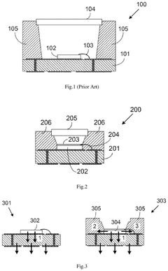
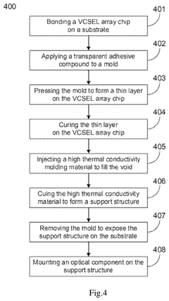
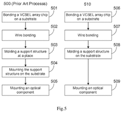
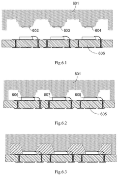
- A VCSEL array package design that includes a VCSEL array chip bonded on a substrate with a support structure molded from high thermal conductivity material, covering the side surfaces of the chip to create additional thermal paths and eliminate gaps, and a transparent thin layer to prevent beam obstruction and reflection.
Thermal Management Strategies
Thermal management represents a critical challenge in VCSEL array packaging for optical neural network accelerators. As power densities increase with higher integration levels, effective heat dissipation becomes essential for maintaining performance, reliability, and longevity of these photonic devices. Current VCSEL arrays in neural network accelerators can generate heat fluxes exceeding 500 W/cm², necessitating sophisticated thermal management approaches.
Passive cooling strategies employ materials with high thermal conductivity to facilitate heat transfer away from active regions. Diamond-based submounts have emerged as premium solutions, offering thermal conductivity up to 2000 W/m·K, significantly outperforming traditional copper (400 W/m·K) or aluminum nitride (170 W/m·K) substrates. Advanced thermal interface materials (TIMs) with embedded graphene or carbon nanotubes further enhance thermal pathways between VCSELs and heat sinks.
Active cooling technologies provide more dynamic thermal management capabilities. Microchannel liquid cooling systems integrated directly into VCSEL array packages have demonstrated the ability to handle heat fluxes up to 1000 W/cm². These systems utilize microfluidic channels as small as 50-100 μm in width to circulate coolants in close proximity to heat sources. Thermoelectric coolers (TECs) offer another active approach, providing precise temperature control through the Peltier effect, though with efficiency penalties.
Thermal design optimization through computational fluid dynamics (CFD) modeling has become standard practice in advanced VCSEL packaging. These simulations enable engineers to identify hotspots and optimize heat spreader geometries before physical prototyping. Recent developments in machine learning algorithms have enhanced these models, reducing simulation time while improving accuracy in predicting thermal behavior under various operating conditions.
Novel packaging architectures specifically addressing thermal concerns include vertically integrated cooling structures where heat sinks are directly bonded to VCSEL arrays, eliminating intermediate thermal resistances. 3D heterogeneous integration approaches place cooling elements in the same package as optical and electronic components, creating more thermally efficient systems. Some cutting-edge designs incorporate phase-change materials that absorb heat during state transitions, providing thermal buffering during peak operation periods.
Industry benchmarks indicate that effective thermal management can extend VCSEL array lifetime by 3-5x and improve wall-plug efficiency by up to 30%. As optical neural network accelerators continue to advance, thermal management strategies will increasingly determine performance ceilings and practical deployment capabilities of these systems in data centers and edge computing applications.
Manufacturing Scalability Assessment
The manufacturing scalability of VCSEL array packaging for optical neural network accelerators represents a critical factor in determining commercial viability and widespread adoption. Current manufacturing processes demonstrate varying degrees of scalability, with established semiconductor packaging techniques providing a foundation for VCSEL array integration. The primary manufacturing approaches include flip-chip bonding, through-silicon vias (TSVs), and wafer-level packaging, each offering distinct advantages for high-volume production.
Flip-chip bonding has emerged as the predominant method for VCSEL array packaging, allowing for direct electrical connections between the VCSEL die and substrate with minimal parasitic effects. This technique achieves approximately 90% yield rates in mature production environments, though maintaining consistent solder bump uniformity across large arrays remains challenging. The process can be scaled to handle arrays containing thousands of individual VCSELs, making it suitable for neural network accelerator applications requiring high element counts.
Wafer-level packaging offers significant cost advantages at scale, potentially reducing per-unit packaging costs by 40-60% compared to individual die packaging. This approach enables simultaneous processing of multiple VCSEL arrays, streamlining testing and quality control procedures. However, thermal management becomes increasingly complex as array density increases, requiring sophisticated heat dissipation solutions that add manufacturing complexity.
Equipment utilization represents another key scalability factor. Current semiconductor packaging equipment can be adapted for VCSEL array production with moderate modifications, avoiding the need for entirely new manufacturing infrastructure. Leading manufacturers report equipment utilization rates of 65-75% for VCSEL packaging lines, indicating room for efficiency improvements as production volumes increase.
Supply chain considerations also impact manufacturing scalability. The specialized materials required for VCSEL packaging, including high-thermal-conductivity substrates and optical-grade encapsulants, may face supply constraints as production volumes increase. Diversification of supplier networks and development of alternative materials will be essential to support large-scale manufacturing operations.
Labor requirements for VCSEL array packaging have decreased by approximately 30% over the past five years due to increased automation, though skilled technicians remain necessary for quality control and process optimization. Training programs and workforce development initiatives will be crucial to address potential labor shortages as manufacturing scales up.
The transition from prototype to high-volume manufacturing represents a significant challenge, with yield rates typically dropping 15-25% during initial scale-up before process optimization. Manufacturers implementing comprehensive statistical process control systems have demonstrated faster yield recovery, typically achieving stable production within 6-9 months of scale-up initiation.
Unlock deeper insights with PatSnap Eureka Quick Research — get a full tech report to explore trends and direct your research. Try now!
Generate Your Research Report Instantly with AI Agent
Supercharge your innovation with PatSnap Eureka AI Agent Platform!