

High-Throughput VCSEL Packaging Line Design
AUG 27, 20259 MIN READ
Generate Your Research Report Instantly with AI Agent
Patsnap Eureka helps you evaluate technical feasibility & market potential.
VCSEL Packaging Evolution and Objectives
Vertical-Cavity Surface-Emitting Lasers (VCSELs) have undergone significant evolution since their inception in the late 1970s. Initially developed as laboratory curiosities, these semiconductor laser diodes have transformed into critical components for various applications including data communications, sensing, and consumer electronics. The packaging technology for VCSELs has evolved from basic TO-can packages to sophisticated array configurations capable of supporting multiple emitters with precise optical alignment.
The early 2000s marked a pivotal shift in VCSEL packaging approaches, transitioning from single-emitter designs to arrays that could support higher power outputs and more complex beam patterns. This evolution was primarily driven by emerging applications in 3D sensing, facial recognition, and automotive LiDAR systems, which demanded greater power density and reliability from VCSEL components.
Traditional VCSEL packaging methods have been characterized by labor-intensive processes including die attachment, wire bonding, and optical alignment, resulting in limited throughput and higher production costs. These constraints have become increasingly problematic as market demand for VCSEL-enabled devices has surged, particularly in smartphone and automotive sectors where annual volume requirements now reach billions of units.
The primary objective of high-throughput VCSEL packaging line design is to dramatically increase production capacity while maintaining or improving quality metrics and reducing per-unit costs. This necessitates a fundamental rethinking of the packaging workflow, incorporating advanced automation, in-line testing, and novel materials handling approaches to overcome current bottlenecks.
Key technical goals include achieving packaging throughputs exceeding 10,000 units per hour, reducing optical alignment times from minutes to seconds, implementing real-time quality monitoring systems, and developing packaging architectures compatible with heterogeneous integration of VCSELs with photodetectors and driver electronics.
Additional objectives focus on environmental sustainability through reduced material waste, lower energy consumption per packaged device, and the development of lead-free packaging solutions that comply with global environmental regulations while maintaining thermal performance and reliability standards.
The evolution trajectory points toward wafer-level packaging techniques that could potentially revolutionize VCSEL manufacturing by enabling simultaneous packaging of thousands of devices, similar to advancements seen in CMOS image sensor production. This approach represents a paradigm shift from discrete device handling to wafer-scale processing that could yield order-of-magnitude improvements in throughput and cost structure.
Market Demand Analysis for High-Throughput VCSEL Solutions
The VCSEL (Vertical-Cavity Surface-Emitting Laser) market has experienced significant growth in recent years, driven primarily by increasing adoption in consumer electronics, particularly in 3D sensing applications for facial recognition systems in smartphones and other mobile devices. Market research indicates that the global VCSEL market size was valued at approximately $2.1 billion in 2020 and is projected to reach $5.3 billion by 2026, representing a compound annual growth rate (CAGR) of 17.3% during the forecast period.
The demand for high-throughput VCSEL packaging solutions is particularly strong due to several converging market factors. First, the proliferation of smartphones with facial recognition capabilities has created a massive demand for VCSEL arrays, with major manufacturers requiring millions of units per quarter. Apple's introduction of Face ID technology in 2017 marked a turning point, establishing VCSELs as a critical component in consumer electronics and creating unprecedented volume requirements.
Beyond smartphones, the automotive industry represents an emerging high-growth market for VCSEL technology. Advanced driver-assistance systems (ADAS) and autonomous driving applications require sophisticated LiDAR systems, many of which utilize VCSEL arrays. Industry forecasts suggest that the automotive VCSEL market segment will grow at a CAGR of 31% through 2025, outpacing the overall VCSEL market growth.
Industrial automation and robotics constitute another significant market driver. Machine vision systems increasingly incorporate VCSEL-based 3D sensing for precise object detection, measurement, and quality control. The industrial automation sector is expected to consume approximately 15% of global VCSEL production by 2024, up from 8% in 2019.
Consumer device manufacturers are demanding increasingly complex VCSEL arrays with higher power outputs and more sophisticated packaging solutions. The average number of elements per VCSEL array has increased from 4-8 elements in 2018 to 16-32 elements in current designs, with some advanced applications requiring arrays with 64 or more elements. This trend necessitates more sophisticated packaging techniques that can maintain alignment precision while handling larger arrays.
Cost pressures remain intense across all market segments. Current VCSEL packaging processes often represent 60-70% of total component cost, creating strong economic incentives for high-throughput packaging solutions that can reduce unit costs. Major smartphone manufacturers have set aggressive cost reduction targets of 15-20% annually for VCSEL components, making packaging efficiency improvements essential for suppliers to remain competitive.
The market clearly signals that manufacturers capable of delivering high-volume, high-precision VCSEL packaging at competitive price points will capture significant market share. This creates a compelling business case for investment in advanced high-throughput VCSEL packaging line design and implementation.
Current VCSEL Packaging Technologies and Bottlenecks
VCSEL (Vertical-Cavity Surface-Emitting Laser) packaging technologies have evolved significantly over the past decade, yet several critical bottlenecks remain in achieving truly high-throughput manufacturing processes. Current packaging approaches can be categorized into three primary methodologies: TO-can packaging, chip-on-board (COB) integration, and wafer-level packaging (WLP).
TO-can packaging represents the traditional approach, offering excellent hermeticity and thermal management. However, this method involves multiple sequential processes including die attach, wire bonding, lid sealing, and testing—each requiring precise alignment and handling. The inherent serial nature of these operations creates a significant throughput limitation, with cycle times typically ranging from 20-30 seconds per device.
Chip-on-board technology has emerged as a more efficient alternative, allowing direct mounting of VCSEL dies onto PCB substrates with integrated electrical connections. While COB enables higher integration density and improved thermal performance, the precision required for accurate die placement (typically ±5μm) creates a production bottleneck. Current pick-and-place equipment struggles to maintain both speed and accuracy at scale.
Wafer-level packaging represents the most promising approach for high-volume production, enabling simultaneous processing of thousands of devices. However, challenges persist in achieving uniform optical performance across the wafer due to stress-induced variations during the packaging process. Additionally, testing capabilities at the wafer level remain limited, often necessitating additional handling steps.
A critical bottleneck across all packaging methodologies is optical alignment. VCSELs require precise positioning relative to optical elements such as lenses or diffusers, with tolerances often below 1μm. Current automated alignment systems operate at speeds incompatible with high-throughput requirements, creating a significant production constraint.
Thermal management presents another substantial challenge. As VCSEL arrays increase in power density, heat dissipation becomes increasingly critical. Current packaging solutions often require complex thermal stacks or heat spreaders that add process steps and handling complexity, further limiting throughput potential.
Testing and quality assurance represent perhaps the most significant bottleneck in the VCSEL packaging process. Current methodologies typically require individual device testing for optical power, beam profile, wavelength stability, and reliability parameters. These tests are predominantly performed serially, with each device requiring 5-15 seconds of testing time—a substantial limitation for high-volume production.
Material handling automation between process steps also remains underdeveloped compared to other semiconductor packaging operations. The delicate nature of VCSEL devices, combined with their optical sensitivity, requires specialized handling solutions that have not yet achieved the speed and reliability necessary for truly high-throughput operations.
State-of-the-Art High-Throughput Packaging Methodologies
01 Automated VCSEL packaging systems
Automated systems for VCSEL packaging significantly improve production line throughput. These systems incorporate robotic handling, automated alignment, and precision mounting technologies to reduce manual intervention and increase processing speed. Advanced automation solutions include integrated testing stations, vision systems for quality control, and synchronized multi-stage operations that optimize the overall packaging workflow.- Automated VCSEL packaging systems: Automated systems for VCSEL packaging significantly improve production line throughput. These systems incorporate advanced handling mechanisms, precise alignment tools, and automated testing procedures to streamline the packaging process. By reducing manual intervention and implementing parallel processing techniques, these automated solutions can substantially increase the number of VCSEL devices packaged per hour while maintaining quality standards.
- Advanced alignment and bonding techniques: Specialized alignment and bonding techniques are crucial for optimizing VCSEL packaging throughput. These include precision optical alignment systems, rapid die bonding methods, and advanced wire bonding technologies that ensure accurate positioning while minimizing cycle time. The implementation of these techniques allows for faster processing speeds and higher yield rates in VCSEL packaging lines, directly contributing to increased throughput.
- Thermal management solutions for high-volume production: Effective thermal management solutions are essential for maintaining high throughput in VCSEL packaging lines. These include innovative heat sink designs, thermal interface materials, and cooling systems that efficiently dissipate heat during continuous operation. By preventing thermal-related failures and downtime, these solutions enable packaging lines to operate at maximum capacity for extended periods, thereby increasing overall throughput.
- Parallel processing and modular packaging approaches: Parallel processing and modular approaches to VCSEL packaging significantly enhance production throughput. These methods involve simultaneous processing of multiple devices, batch handling systems, and modular line configurations that can be scaled according to production demands. By processing multiple VCSEL components concurrently rather than sequentially, these approaches can multiply the effective throughput of packaging lines.
- Quality control and testing integration: Integrated quality control and testing systems are vital for maintaining high throughput in VCSEL packaging lines. These include in-line optical inspection tools, automated electrical testing equipment, and real-time monitoring systems that detect defects early in the packaging process. By reducing the need for separate testing stages and minimizing rework, these integrated approaches ensure that high throughput does not come at the expense of product quality.
02 Thermal management in high-throughput VCSEL packaging
Effective thermal management is crucial for maintaining high throughput in VCSEL packaging lines. Innovative heat dissipation techniques, including advanced substrate materials, integrated heat sinks, and thermal interface materials, enable faster processing speeds without compromising device reliability. These solutions prevent thermal-induced failures during high-volume production and ensure consistent performance of packaged VCSELs.Expand Specific Solutions03 Parallel processing techniques for VCSEL packaging
Parallel processing techniques substantially increase VCSEL packaging line throughput by enabling simultaneous handling of multiple devices. These methods include array-based packaging approaches, batch processing systems, and multi-channel testing equipment. By processing multiple VCSELs concurrently rather than sequentially, manufacturing efficiency is significantly improved while maintaining quality standards.Expand Specific Solutions04 Advanced optical alignment systems for high-speed VCSEL packaging
Precision optical alignment systems are essential for maximizing VCSEL packaging throughput. These systems incorporate real-time feedback mechanisms, automated positioning algorithms, and high-precision actuators to achieve rapid and accurate alignment. Advanced technologies such as machine vision, laser interferometry, and active alignment systems reduce alignment time while ensuring optimal coupling efficiency and device performance.Expand Specific Solutions05 Quality control integration for efficient VCSEL packaging
Integrated quality control systems enhance VCSEL packaging line throughput by reducing bottlenecks associated with separate testing processes. In-line inspection technologies, real-time monitoring systems, and automated defect detection capabilities enable immediate identification of issues without interrupting the production flow. These systems incorporate optical performance testing, electrical parameter verification, and structural integrity checks that maintain high quality standards while optimizing production speed.Expand Specific Solutions
Key Industry Players in VCSEL Manufacturing Ecosystem
The VCSEL packaging high-throughput line design market is currently in a growth phase, with increasing demand driven by data centers, 3D sensing, and automotive applications. The global market is projected to reach significant scale as VCSEL technology matures from early adoption to mainstream implementation. Leading players include established semiconductor giants like Intel and Micron Technology, alongside specialized optical component manufacturers such as Mellanox Technologies and Coherent (formerly II-VI). Chinese companies including Fujian Huixin Laser and Vertilite are rapidly advancing their technological capabilities, particularly in high-speed optical chips for AI applications. The competitive landscape shows regional clusters of expertise forming in the US, Europe, and Asia, with companies differentiating through proprietary packaging techniques, automation levels, and integration capabilities.
II-VI Delaware, Inc.
Technical Solution: II-VI has developed an advanced high-throughput VCSEL packaging line that integrates automated optical alignment systems with real-time feedback control. Their solution employs a multi-stage approach where VCSELs are first precision-mounted on submounts using automated die bonders with placement accuracy of <1μm. The company utilizes proprietary high-speed testing stations that can characterize thousands of devices per hour, performing both electrical and optical measurements simultaneously. Their packaging line incorporates in-situ process monitoring with machine vision systems that detect defects at multiple stages, reducing downstream failures. II-VI's approach includes automated wire bonding stations with multi-head capabilities that can process up to 8 devices simultaneously, significantly increasing throughput compared to traditional single-head systems. The company has also implemented advanced thermal management solutions during the packaging process to ensure consistent device performance and reliability.
Strengths: Industry-leading throughput rates with demonstrated capacity exceeding 50 million units annually; exceptional placement accuracy leading to higher yields; integrated quality control systems reducing downstream failures. Weaknesses: Higher initial capital investment compared to semi-automated solutions; requires specialized maintenance personnel; system complexity can lead to longer setup times when changing product specifications.
Sanhe Laserconn Tech Co. Ltd.
Technical Solution: Sanhe Laserconn has developed an innovative high-throughput VCSEL packaging solution called "LaserLine" that emphasizes process integration and yield optimization. Their system employs a linear manufacturing concept where devices progress through interconnected process chambers with automated transfer mechanisms, minimizing handling-related damage. The solution incorporates high-precision die placement using vision-guided robotics achieving positioning accuracy of approximately 1μm. Sanhe's approach features integrated in-line testing at multiple process stages, including pre-bond electrical verification, post-bond optical characterization, and final package validation, enabling early detection of defects. Their packaging line utilizes specialized micro-welding techniques for electrical connections that minimize thermal stress compared to traditional wire bonding. The company has implemented advanced environmental controls throughout the manufacturing process, maintaining Class 100 cleanroom conditions in critical areas to reduce contamination-related failures. Sanhe's system includes automated optical inspection with machine learning algorithms that continuously improve defect recognition capabilities based on production data.
Strengths: Highly integrated process flow reducing handling-related damage and contamination; excellent yield rates exceeding 98% in production environments; competitive pricing making the technology accessible to growing manufacturers. Weaknesses: More limited customization options compared to modular systems from larger competitors; somewhat lower throughput rates (approximately 30 million units annually); less extensive global support infrastructure for maintenance and upgrades.
Critical Patents and Innovations in VCSEL Packaging
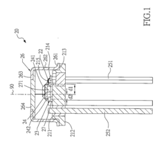
Packaging assembly for high-speed vertical-cavity surface-emitting laser
PatentInactiveTW201914135A
Innovation
- A high-speed vertical resonant cavity surface-emitting laser packaging structure that uses a lens assembly to split laser light, guiding a portion back to a monitor photodetector and positioning the laser element closer to the pins, reducing signal loss and minimizing reflected light interference.
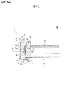
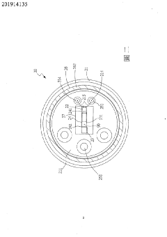
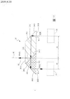
Packaging Assembly for High-Speed Vertical-Cavity Surface-Emitting Laser
PatentActiveUS20190081455A1
Innovation
- A packaging assembly that uses a lens assembly with a half-reflecting, half-transmitting surface to split the laser beam, directing a portion to a monitor photodiode and allowing the VCSEL element to be positioned closer to the pins, thereby shortening bonding wires and reducing signal loss.

Cost-Benefit Analysis of Production Line Scaling
The scaling of VCSEL packaging production lines presents significant economic considerations that must be carefully evaluated. Initial capital expenditure for high-throughput VCSEL packaging equipment represents a substantial investment, typically ranging from $2-5 million for a fully automated line. However, this investment can be justified through increased production capacity, which may reach 10,000-15,000 units per day compared to 2,000-3,000 units with conventional methods.
Labor cost reduction constitutes a primary benefit of scaled production, with automated systems requiring only 2-3 operators per shift versus 8-10 for manual operations. This translates to approximately 70% reduction in direct labor costs over a five-year operational period. Additionally, quality improvements from automation reduce scrap rates from typical 5-7% to below 2%, representing significant material conservation and yield enhancement.
Energy efficiency improvements also contribute to operational savings, with modern high-throughput systems consuming 30-40% less power per unit produced compared to traditional batch processing methods. The integration of real-time monitoring systems further reduces maintenance costs by enabling predictive maintenance protocols, decreasing unplanned downtime by up to 60%.
Return on investment calculations indicate that most high-throughput VCSEL packaging lines achieve breakeven within 18-24 months under standard production volumes. This timeline can be accelerated to 12-15 months when operating at maximum capacity. Sensitivity analysis shows that production volume is the most critical factor affecting ROI, with a 20% decrease in volume potentially extending payback periods by 6-8 months.
Scalability considerations reveal that modular line designs offer superior long-term value, allowing incremental capacity expansion at approximately 60% of the cost of new line installation. This approach provides flexibility to adapt to market demand fluctuations while optimizing capital utilization. Furthermore, economies of scale become evident when production exceeds 5 million units annually, with per-unit packaging costs decreasing by 15-20%.
Risk assessment indicates that market volatility represents the primary threat to investment recovery, particularly in consumer electronics applications where product lifecycles are shortening. Diversification across multiple VCSEL applications (sensing, data communication, automotive) can mitigate this risk by ensuring consistent production volumes despite fluctuations in individual market segments.
Quality Control Systems for High-Volume VCSEL Manufacturing
Quality control systems represent a critical component in high-volume VCSEL manufacturing environments, particularly when designing high-throughput packaging lines. These systems must ensure consistent performance while maintaining production efficiency across thousands of devices per hour.
Advanced optical inspection systems form the foundation of modern VCSEL quality control. These systems employ high-resolution cameras and specialized lighting to detect surface defects, misalignments, and contamination at submicron levels. Machine vision algorithms analyze these images in real-time, flagging potential issues without impacting throughput rates.
In-line spectral analysis has become increasingly important for VCSEL quality assurance. Automated spectrometers measure key parameters including wavelength accuracy, spectral width, and power distribution across the emission profile. These measurements occur at multiple stages throughout the packaging process, allowing for early detection of performance drift before final assembly.
Thermal profiling systems monitor temperature stability during critical bonding processes. Infrared cameras and embedded thermal sensors track heat distribution across the packaging line, ensuring optimal curing conditions for adhesives and preventing thermal stress that could compromise device reliability. Data from these systems feeds into statistical process control algorithms that can predict potential failures before they occur.
Automated electrical testing represents another crucial quality control element. High-speed test fixtures verify electrical characteristics including threshold current, slope efficiency, and forward voltage at production speeds. Advanced systems incorporate parallel testing capabilities, simultaneously evaluating multiple devices to maintain throughput targets while ensuring 100% functional verification.
Traceability systems integrate with quality control infrastructure to maintain comprehensive device histories. Each VCSEL receives a unique identifier, with all test data, process parameters, and inspection results linked to this ID. This enables detailed failure analysis and continuous process improvement while satisfying regulatory requirements in medical and automotive applications.
Machine learning algorithms increasingly enhance quality control capabilities by identifying subtle patterns that precede device failures. These systems analyze historical production data to establish correlations between process variations and performance outcomes, enabling predictive maintenance and process optimization that reduces both scrap rates and downtime.
Unlock deeper insights with Patsnap Eureka Quick Research — get a full tech report to explore trends and direct your research. Try now!
Generate Your Research Report Instantly with AI Agent
Supercharge your innovation with Patsnap Eureka AI Agent Platform!