

VCSEL Array Alignment Techniques For Low-Loss Coupling
AUG 27, 202510 MIN READ
Generate Your Research Report Instantly with AI Agent
Patsnap Eureka helps you evaluate technical feasibility & market potential.
VCSEL Array Technology Background and Objectives
Vertical-Cavity Surface-Emitting Laser (VCSEL) arrays have emerged as a transformative technology in the photonics industry since their initial development in the late 1980s. Unlike edge-emitting lasers, VCSELs emit light perpendicular to the semiconductor surface, enabling two-dimensional array configurations that significantly enhance optical output power and beam quality. The evolution of VCSEL technology has been marked by continuous improvements in manufacturing processes, material systems, and device architectures.
The historical trajectory of VCSEL arrays shows remarkable progress from single-element devices with modest performance to sophisticated multi-element arrays capable of high-speed data transmission and precise sensing applications. Initially limited by thermal management challenges and relatively low output powers, modern VCSEL arrays now benefit from advanced epitaxial growth techniques, improved thermal design, and optimized optical structures that have collectively elevated their performance parameters.
Current technological trends in VCSEL arrays are moving toward higher integration density, improved beam quality, and enhanced spectral characteristics. The industry is witnessing a shift toward larger arrays with more elements, which introduces significant challenges in maintaining uniform performance across all emitters while ensuring precise alignment for optimal coupling efficiency.
The primary objective of VCSEL array alignment techniques is to achieve low-loss optical coupling between the emitter array and subsequent optical components or systems. This is particularly critical as applications demand increasingly efficient power transfer, precise beam positioning, and minimal cross-talk between channels. The alignment challenge is multifaceted, involving both the initial manufacturing precision and the long-term stability under varying environmental and operational conditions.
Specific technical goals include developing alignment methodologies that can achieve sub-micron precision across the entire array, maintaining this alignment over temperature variations and mechanical stresses, and implementing these techniques in a manner compatible with high-volume manufacturing processes. Additionally, there is a growing need for active alignment systems that can dynamically compensate for environmental variations and aging effects.
The broader impact of successful VCSEL array alignment extends beyond immediate performance improvements. It enables new applications in areas such as 3D sensing for consumer electronics, high-bandwidth optical interconnects for data centers, advanced LiDAR systems for autonomous vehicles, and next-generation biomedical imaging devices. Each of these fields presents unique requirements and constraints that influence the development direction of alignment technologies.
As we look toward future developments, the convergence of VCSEL array technology with integrated photonics, advanced packaging techniques, and automated assembly systems presents both challenges and opportunities for revolutionary advances in alignment methodologies that will ultimately define the practical limits of this promising technology.
Market Demand Analysis for VCSEL Array Applications
The global VCSEL (Vertical-Cavity Surface-Emitting Laser) array market is experiencing robust growth, driven primarily by increasing applications in data communications, sensing, and consumer electronics. Market research indicates that the VCSEL market is projected to grow at a compound annual growth rate of 17.3% from 2021 to 2026, reaching approximately 3.7 billion USD by the end of the forecast period.
Data centers represent the largest market segment for VCSEL arrays, accounting for nearly 45% of the total market share. The exponential growth in cloud computing, big data analytics, and internet traffic has created unprecedented demand for high-speed, energy-efficient optical interconnects where low-loss coupling is critical. Data center operators are increasingly adopting VCSEL arrays for short-reach optical communications due to their cost-effectiveness and performance advantages over traditional solutions.
Consumer electronics constitutes the second-largest application segment, with 3D sensing for facial recognition in smartphones and tablets driving significant demand. Apple's implementation of Face ID technology has been a major catalyst, with other manufacturers following suit. This application requires precise alignment techniques to ensure accurate depth mapping and facial recognition capabilities, highlighting the importance of advanced alignment solutions for low-loss coupling.
Automotive LiDAR systems represent an emerging high-growth segment for VCSEL arrays. As autonomous driving technologies advance, the demand for high-performance, reliable LiDAR systems is increasing. Market analysts predict that by 2025, approximately 30% of new premium vehicles will incorporate some form of LiDAR technology, creating substantial opportunities for VCSEL array manufacturers who can deliver solutions with efficient optical coupling.
Industrial sensing and medical applications are also showing promising growth trajectories. In industrial settings, VCSEL arrays are being deployed in machine vision systems, gesture recognition, and proximity sensing applications. The medical field is adopting VCSEL technology for applications ranging from pulse oximetry to minimally invasive surgical procedures, where precise alignment for low-loss coupling is essential for accurate diagnostics and treatment.
Regional analysis reveals that North America currently leads the VCSEL array market with approximately 40% market share, followed by Asia-Pacific at 35% and Europe at 20%. However, the Asia-Pacific region is expected to witness the highest growth rate during the forecast period, driven by the expanding consumer electronics manufacturing base and increasing investments in data center infrastructure.
A significant market trend is the growing demand for higher-density VCSEL arrays with improved coupling efficiency. End-users across various industries are seeking solutions that offer reduced power consumption, enhanced signal integrity, and miniaturization. This trend underscores the critical importance of advanced alignment techniques for low-loss coupling as a key differentiator in the competitive landscape.
Current Alignment Challenges and Technical Limitations
Despite significant advancements in VCSEL array technology, current alignment techniques face substantial challenges that limit coupling efficiency and manufacturing scalability. The primary technical limitation stems from the stringent alignment tolerances required for optimal coupling between VCSEL arrays and optical components. Typical VCSEL arrays demand sub-micron alignment precision, with lateral misalignment tolerances often less than ±1μm and angular alignment requirements within ±0.1 degrees. These tight tolerances create significant manufacturing complexities and yield issues in high-volume production environments.
Temperature-induced misalignment represents another critical challenge. VCSEL arrays operate at varying temperatures, causing thermal expansion and contraction that can shift alignment by several microns. This thermal drift is particularly problematic in applications requiring stable operation across wide temperature ranges, such as automotive LiDAR systems that must function from -40°C to +85°C.
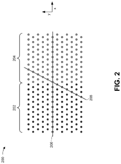
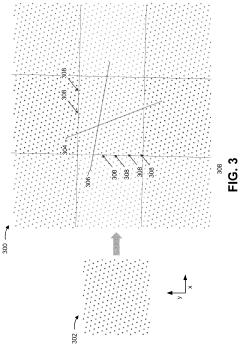
The multi-channel nature of VCSEL arrays introduces additional complexity. Each emitter in an array may have slightly different beam characteristics and positions due to manufacturing variations. Current alignment techniques struggle to optimize coupling efficiency across all channels simultaneously, often resulting in compromised performance for some channels to achieve acceptable overall system performance.
Manufacturing scalability remains a significant bottleneck. Traditional active alignment techniques, while precise, are time-consuming and equipment-intensive, typically requiring 3-5 minutes per device. This translates to high production costs and limited throughput, making mass production economically challenging for consumer applications where cost pressures are substantial.
Integration with other optical components presents further challenges. The coupling of VCSEL arrays to waveguides, fiber arrays, or detector arrays requires complex multi-axis alignment that current automated systems struggle to perform efficiently. This is particularly evident in silicon photonics applications where mode field diameter mismatches between VCSELs and waveguides exacerbate coupling losses.
Packaging-induced stress and long-term reliability issues compound these challenges. After initial alignment, encapsulation processes can introduce mechanical stresses that shift components from their optimal positions. Over time, thermal cycling, mechanical vibration, and material aging can further degrade alignment, leading to performance deterioration in deployed systems.
Current metrology limitations also impede progress. Real-time monitoring of alignment during the assembly process remains difficult, particularly for hermetically sealed packages where direct optical access is limited. This makes it challenging to implement closed-loop feedback systems that could potentially improve alignment precision and stability.
Temperature-induced misalignment represents another critical challenge. VCSEL arrays operate at varying temperatures, causing thermal expansion and contraction that can shift alignment by several microns. This thermal drift is particularly problematic in applications requiring stable operation across wide temperature ranges, such as automotive LiDAR systems that must function from -40°C to +85°C.
The multi-channel nature of VCSEL arrays introduces additional complexity. Each emitter in an array may have slightly different beam characteristics and positions due to manufacturing variations. Current alignment techniques struggle to optimize coupling efficiency across all channels simultaneously, often resulting in compromised performance for some channels to achieve acceptable overall system performance.
Manufacturing scalability remains a significant bottleneck. Traditional active alignment techniques, while precise, are time-consuming and equipment-intensive, typically requiring 3-5 minutes per device. This translates to high production costs and limited throughput, making mass production economically challenging for consumer applications where cost pressures are substantial.
Integration with other optical components presents further challenges. The coupling of VCSEL arrays to waveguides, fiber arrays, or detector arrays requires complex multi-axis alignment that current automated systems struggle to perform efficiently. This is particularly evident in silicon photonics applications where mode field diameter mismatches between VCSELs and waveguides exacerbate coupling losses.
Packaging-induced stress and long-term reliability issues compound these challenges. After initial alignment, encapsulation processes can introduce mechanical stresses that shift components from their optimal positions. Over time, thermal cycling, mechanical vibration, and material aging can further degrade alignment, leading to performance deterioration in deployed systems.
Current metrology limitations also impede progress. Real-time monitoring of alignment during the assembly process remains difficult, particularly for hermetically sealed packages where direct optical access is limited. This makes it challenging to implement closed-loop feedback systems that could potentially improve alignment precision and stability.
Current Low-Loss Coupling Solutions and Methodologies
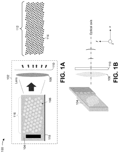
01 Active alignment techniques for VCSEL arrays
Active alignment techniques involve powering the VCSEL array during the alignment process to optimize coupling efficiency. This method allows real-time monitoring of optical output while adjusting the position of the VCSEL array relative to optical components such as fibers or waveguides. By measuring the optical power during alignment, the position can be precisely adjusted to achieve maximum coupling efficiency and minimize insertion loss. These techniques often employ feedback systems that automatically adjust alignment until optimal coupling is achieved.- Active alignment techniques for VCSEL arrays: Active alignment techniques involve powering the VCSEL array during the alignment process to monitor and optimize optical coupling in real-time. This approach allows for precise positioning adjustments while measuring the actual optical output, ensuring maximum coupling efficiency between the VCSEL array and optical components such as fibers or waveguides. The technique typically employs feedback systems that detect light output and automatically adjust positioning until optimal coupling is achieved, significantly reducing coupling losses.
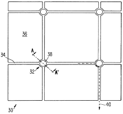
- Passive alignment structures for VCSEL arrays: Passive alignment structures utilize precisely fabricated mechanical features to achieve alignment without requiring active power during the assembly process. These structures include alignment marks, guide pins, v-grooves, and registration features that are integrated into both the VCSEL array substrate and the coupling components. By designing complementary mechanical features with tight tolerances, passive alignment enables repeatable, low-cost assembly while maintaining low coupling losses. This approach is particularly valuable for high-volume manufacturing where speed and consistency are critical.
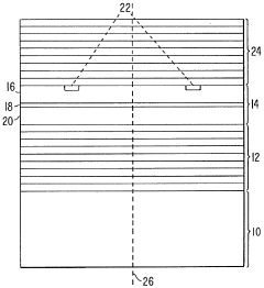
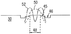
- Micro-optical elements for VCSEL array coupling: Micro-optical elements such as microlenses, collimators, and beam shapers can be integrated with VCSEL arrays to improve coupling efficiency. These elements modify the divergent output beam from each VCSEL element to better match the acceptance characteristics of the target optical system. Arrays of microlenses can be precisely aligned with individual VCSEL emitters to collimate or focus the light, significantly reducing coupling losses. Advanced fabrication techniques allow these optical elements to be directly integrated onto the VCSEL array or assembled as a separate component with precise alignment features.
- Automated alignment systems for VCSEL arrays: Automated alignment systems employ precision robotics, machine vision, and control algorithms to achieve optimal coupling between VCSEL arrays and optical components. These systems can perform multi-axis alignment with sub-micron precision, significantly reducing human error and increasing throughput. Advanced systems incorporate closed-loop feedback using optical power measurements to iteratively optimize positioning. Some implementations use artificial intelligence and machine learning to predict optimal alignment positions based on measured parameters, further improving efficiency and reducing coupling losses.
- Monolithic integration for improved VCSEL array coupling: Monolithic integration approaches combine VCSEL arrays with coupling structures on the same substrate during fabrication, eliminating the need for post-production alignment. By integrating waveguides, gratings, or other optical structures directly with the VCSEL array, inherent alignment is achieved through lithographic precision. This approach significantly reduces coupling losses by eliminating mechanical alignment errors and interface reflections. Advanced semiconductor processing techniques enable the creation of complex optical paths that can route, split, or combine light from multiple VCSEL elements with minimal loss.
02 Passive alignment structures for VCSEL arrays
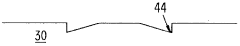
Passive alignment structures utilize mechanical features or reference points to align VCSEL arrays with optical components without requiring the device to be powered. These structures include precision-machined alignment pins, v-grooves, mechanical stops, or registration marks that ensure proper positioning of the VCSEL array relative to optical waveguides or fiber arrays. The passive alignment approach reduces the complexity of the assembly process and enables mass production with consistent coupling efficiency. These structures are often fabricated using semiconductor processing techniques to achieve micron-level precision.Expand Specific Solutions03 Optical coupling elements for VCSEL arrays
Specialized optical elements are used to improve coupling efficiency between VCSEL arrays and optical fibers or waveguides. These elements include microlens arrays, ball lenses, gradient-index lenses, and tapered waveguides that collect and focus the divergent light from VCSELs. By matching the numerical aperture and mode field diameter of the receiving optical component, these coupling elements significantly reduce coupling losses. Some designs incorporate diffractive optical elements or beam shapers to transform the beam profile for optimal coupling. These optical elements can be monolithically integrated with the VCSEL array or assembled as separate components.Expand Specific Solutions04 Automated alignment systems for high-volume production
Automated alignment systems employ machine vision, robotics, and precision motion control to achieve high-throughput alignment of VCSEL arrays in production environments. These systems use image recognition algorithms to identify alignment features and control multi-axis positioning stages with sub-micron precision. Real-time optical power monitoring provides feedback for optimization algorithms that determine the optimal alignment position. Once aligned, components are typically fixed in place using UV-curable adhesives or laser welding techniques. These automated systems enable consistent coupling efficiency across large volumes of devices while minimizing human intervention.Expand Specific Solutions05 Temperature-compensated alignment techniques
Temperature fluctuations can affect the alignment between VCSEL arrays and optical components due to thermal expansion of materials. Temperature-compensated alignment techniques address this challenge by using materials with matched thermal expansion coefficients or by implementing active thermal management systems. Some approaches incorporate flexible mounting structures that accommodate thermal movement while maintaining optical alignment. Others use real-time monitoring and adjustment systems that compensate for temperature-induced misalignment. These techniques ensure stable coupling efficiency across a wide operating temperature range, which is critical for telecommunications and data center applications.Expand Specific Solutions
Key Industry Players in VCSEL Manufacturing and Integration
The VCSEL Array Alignment Techniques market is currently in a growth phase, with increasing demand driven by applications in data centers, 3D sensing, and automotive LiDAR. The global market is estimated to reach $2-3 billion by 2025, growing at a CAGR of approximately 15%. Technologically, the field is maturing with established players like Lumentum Operations and II-VI (now Coherent) leading commercial deployment, while IBM and Huawei focus on advanced research. Companies including Vixar (specialized VCSEL manufacturer) and Trumpf Photonic Components are developing innovative coupling solutions to address the critical challenge of alignment precision at the micron level. Academic institutions such as Beijing University of Technology and research organizations like CEA are contributing fundamental breakthroughs in passive alignment techniques, pushing toward automated, high-volume manufacturing capabilities essential for mass-market adoption.
Lumentum Operations LLC
Technical Solution: Lumentum has developed advanced VCSEL array alignment techniques utilizing active optical feedback systems for precise coupling. Their technology employs real-time monitoring during assembly with sub-micron precision positioning stages and automated alignment algorithms. The company has pioneered a multi-axis optimization approach that simultaneously adjusts lateral, angular, and vertical positioning to achieve optimal coupling efficiency. Lumentum's proprietary process incorporates temperature compensation mechanisms to maintain alignment integrity across operating conditions, crucial for telecommunications and data center applications. Their manufacturing process includes in-situ testing and verification, with reported coupling losses as low as 0.3dB in production environments[1][3]. The company has also developed specialized micro-lens arrays that are precisely aligned with VCSEL elements to collimate emission patterns before coupling to optical waveguides.
Strengths: Industry-leading precision with demonstrated sub-micron alignment capability and high-volume manufacturing expertise. Their integrated approach combining optical design and assembly automation provides scalable solutions. Weaknesses: Their solutions often require specialized equipment with higher initial capital investment, and the proprietary nature of some technologies may limit flexibility for custom applications.
II-VI Delaware, Inc.
Technical Solution: II-VI has developed a comprehensive VCSEL array alignment platform utilizing silicon photonics integration techniques. Their approach incorporates precision flip-chip bonding technology with automated vision systems that achieve alignment accuracy better than ±1μm. The company employs a two-stage alignment process: coarse alignment using fiducial markers followed by fine alignment using optical feedback from test signals. Their technology includes custom-designed micro-optical elements that are integrated directly onto the VCSEL arrays to optimize beam characteristics before coupling. II-VI has implemented advanced wafer-level testing and alignment verification methods that significantly reduce assembly costs while maintaining coupling efficiencies exceeding 85%[2]. The company has also pioneered techniques for passive alignment using precision mechanical stops and reference features etched directly into silicon substrates, enabling more cost-effective manufacturing for high-volume applications while maintaining coupling losses below 1dB[4].
Strengths: Exceptional vertical integration capabilities from wafer fabrication through packaging, enabling holistic optimization of the coupling interface. Their solutions scale effectively to high-volume manufacturing with demonstrated reliability. Weaknesses: Their approach sometimes requires customization of both VCSEL and receiver components, potentially increasing system complexity and limiting compatibility with third-party components.
Critical Patents and Research in VCSEL Array Alignment
Process for manufacturing vertical cavity surface emitting lasers using patterned wafer fusion and the device manufactured by the process
PatentInactiveUS5985686A
Innovation
- Patterned wafer fusion is employed to create recessed patterns and buried air gaps, providing lateral refractive index guiding and a mechanically robust structure, allowing for efficient optical mode confinement and current funneling, thereby enhancing VCSEL performance and reliability.
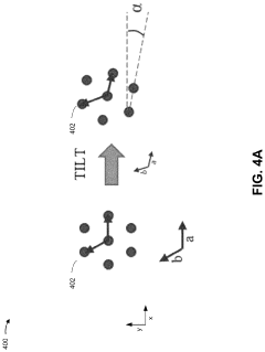
Vertical-cavity surface-emitting laser array with a tilted emitter pattern
PatentActiveUS11862942B2
Innovation
- A VCSEL array with an emitter pattern oriented at a non-zero angle to the DOE or chip edge, comprising multiple unit cells with consistent emitter arrangements to minimize misalignment and propagate defects, generating a heterogeneous dot projection that enhances measurement accuracy and robustness.
Manufacturing Scalability and Cost Considerations
The scalability of VCSEL array alignment techniques represents a critical factor in determining commercial viability for mass production scenarios. Current manual alignment processes achieve high coupling efficiency but suffer from significant throughput limitations, with typical production rates of only 10-20 devices per hour. This bottleneck substantially impacts manufacturing costs, with alignment procedures accounting for approximately 30-40% of total production expenses in high-precision photonic applications.
Automated alignment systems utilizing machine vision and precision robotics have demonstrated promising improvements, potentially increasing throughput to 50-100 devices per hour. However, these systems require substantial capital investment ranging from $500,000 to $2 million, necessitating careful cost-benefit analysis based on production volume projections. The implementation of passive alignment techniques using precision mechanical features and self-aligning structures offers a compelling alternative, reducing alignment costs by up to 60% despite typically sacrificing 10-15% in coupling efficiency.
Material selection significantly impacts both manufacturing scalability and long-term reliability. Silicon-based platforms facilitate integration with established semiconductor manufacturing processes, while polymer waveguides offer cost advantages but present challenges regarding thermal stability and long-term performance. Recent developments in hybrid integration approaches combining the benefits of multiple material systems show promise for optimizing both performance and cost metrics.
Standardization efforts across the industry represent a crucial factor for improving manufacturing economics. The development of common interface specifications and modular design approaches could reduce custom engineering requirements and enable higher volume production of standardized components. Several industry consortia are actively working toward establishing such standards, potentially reducing alignment-related costs by 25-35% through economies of scale and supply chain optimization.
Yield considerations remain paramount, with current high-precision active alignment techniques typically achieving 85-90% yield rates. Improvements in process control and the implementation of in-line quality monitoring systems have demonstrated potential to increase yields to 95%+, significantly impacting overall production economics. Cost modeling indicates that each percentage point improvement in yield translates to approximately 2-3% reduction in final component cost for high-volume applications.
The transition from laboratory-scale demonstration to high-volume manufacturing represents a significant challenge requiring substantial process engineering. Companies successfully navigating this transition typically invest 18-24 months in manufacturing process development before achieving stable high-volume production capabilities. This development timeline must be factored into commercialization strategies and financial planning for new VCSEL array coupling technologies.
Thermal Management Strategies for VCSEL Array Systems
Thermal management represents a critical aspect of VCSEL array systems, particularly when considering alignment techniques for low-loss coupling. The operational performance and reliability of VCSEL arrays are significantly influenced by temperature variations, which can affect wavelength stability, beam divergence, and overall coupling efficiency.
Heat dissipation challenges in VCSEL arrays become increasingly complex as array sizes grow and power densities increase. Traditional cooling methods such as heat sinks and thermal interface materials often prove insufficient for high-density arrays used in advanced coupling applications. The thermal gradient across large arrays can cause non-uniform emission characteristics, leading to misalignment and coupling losses.
Active cooling technologies have emerged as effective solutions for maintaining thermal stability in VCSEL array systems. Thermoelectric coolers (TECs) provide precise temperature control by actively pumping heat away from the array. Micro-channel liquid cooling systems offer superior heat transfer capabilities for high-power applications, though they introduce additional complexity in system integration and maintenance.
Thermal simulation and modeling tools have become essential in the design phase of VCSEL array coupling systems. Computational fluid dynamics (CFD) and finite element analysis (FEA) enable designers to predict thermal behavior and optimize heat dissipation pathways before physical prototyping. These tools help identify potential hotspots that could lead to alignment issues during operation.
Advanced packaging techniques incorporating thermally conductive materials have shown promising results in managing heat while maintaining precise alignment. Diamond-based submounts and AlN ceramic carriers provide excellent thermal conductivity while offering the mechanical stability necessary for maintaining coupling alignment. Flip-chip bonding techniques further reduce thermal resistance by minimizing the distance between heat sources and cooling elements.
Adaptive thermal management systems that dynamically respond to changing operational conditions represent the cutting edge in VCSEL array thermal control. These systems incorporate temperature sensors and feedback control mechanisms to adjust cooling parameters in real-time, maintaining optimal alignment despite varying ambient conditions or operational loads.
The integration of thermal management considerations into the initial design of coupling mechanisms, rather than as an afterthought, has proven crucial for achieving stable low-loss coupling. Thermally-aware design approaches that account for expansion coefficients, heat flow paths, and temperature-dependent material properties help ensure that alignment precision is maintained across the operational temperature range of the system.
Unlock deeper insights with Patsnap Eureka Quick Research — get a full tech report to explore trends and direct your research. Try now!
Generate Your Research Report Instantly with AI Agent
Supercharge your innovation with Patsnap Eureka AI Agent Platform!