Femtosecond Laser Micromachining For VCSEL Integration
AUG 27, 202510 MIN READ
Generate Your Research Report Instantly with AI Agent
Patsnap Eureka helps you evaluate technical feasibility & market potential.
Femtosecond Laser Micromachining Background and Objectives
Femtosecond laser micromachining has emerged as a revolutionary technology in the field of photonics and semiconductor manufacturing, particularly for Vertical-Cavity Surface-Emitting Laser (VCSEL) integration. The evolution of this technology spans over three decades, beginning with the development of ultrafast lasers in the 1990s and progressing to their application in precision micromachining in the early 2000s. The convergence of femtosecond laser technology with VCSEL manufacturing represents a significant technological advancement that addresses critical challenges in photonics integration.
The fundamental principle behind femtosecond laser micromachining lies in its ultrashort pulse duration, typically ranging from 30 to 1000 femtoseconds. These ultrashort pulses enable non-thermal material removal through multiphoton absorption and plasma formation, resulting in minimal heat-affected zones and unprecedented precision at the submicron scale. This characteristic makes femtosecond lasers particularly suitable for processing delicate semiconductor materials used in VCSEL fabrication.
Recent technological trends indicate a growing emphasis on improving the throughput and reliability of femtosecond laser systems for industrial applications. Advancements in beam delivery systems, pulse shaping techniques, and control algorithms have significantly enhanced the capability of these systems to perform complex micromachining tasks required for VCSEL integration. The development of high-repetition-rate femtosecond lasers has also contributed to increased processing speeds, making the technology more economically viable for mass production.
The primary technical objectives for femtosecond laser micromachining in VCSEL integration encompass several critical areas. First, achieving precise and repeatable feature sizes below 1 μm is essential for creating optical waveguides and coupling structures. Second, maintaining material integrity during processing is crucial to preserve the optical and electrical properties of the semiconductor materials. Third, developing efficient strategies for three-dimensional structuring enables the creation of complex photonic integrated circuits incorporating VCSELs.
Another significant objective is the seamless integration of femtosecond laser processing into existing semiconductor manufacturing workflows. This requires developing compatible process parameters, establishing reliable quality control methods, and ensuring consistency across large-scale production. Additionally, reducing the overall processing time and cost remains a persistent goal to enhance the commercial viability of this technology.
Looking forward, the technology aims to enable novel VCSEL architectures that were previously unattainable with conventional fabrication methods. These include high-density VCSEL arrays with integrated optical interconnects, beam-steering capabilities, and on-chip sensing functionalities. The ultimate goal is to establish femtosecond laser micromachining as a standard tool in the photonics industry for creating next-generation integrated photonic devices centered around VCSEL technology.
Market Demand for VCSEL Integration Solutions
The VCSEL (Vertical-Cavity Surface-Emitting Laser) market has experienced significant growth in recent years, driven primarily by increasing applications in data communications, sensing, and consumer electronics. The global VCSEL market was valued at approximately $2.1 billion in 2020 and is projected to reach $5.3 billion by 2026, representing a compound annual growth rate (CAGR) of over 17%.
Integration solutions for VCSELs have become particularly crucial as device miniaturization continues across multiple industries. The smartphone industry represents one of the largest demand drivers, with 3D sensing applications for facial recognition and augmented reality features requiring increasingly compact and efficient VCSEL arrays. Apple's implementation of Face ID technology alone has driven substantial market growth, with each iPhone incorporating multiple VCSEL components.
Automotive LiDAR systems represent another rapidly expanding market segment, expected to grow at a CAGR of 34% through 2025. These systems require precise integration of VCSEL arrays with optical components to achieve the performance necessary for autonomous driving applications. The demand for higher resolution, longer range, and more compact LiDAR systems is pushing manufacturers toward advanced integration solutions.
Data center applications constitute a third major market driver, with the increasing bandwidth requirements necessitating higher-density optical interconnects. The transition to 400G and 800G data rates is accelerating the adoption of VCSEL arrays in short-reach optical links, creating demand for integration technologies that can maintain signal integrity while reducing form factors.
Industry surveys indicate that over 65% of VCSEL manufacturers identify integration challenges as a significant barrier to meeting customer requirements. Traditional integration methods often involve multiple process steps, increasing production costs and reducing yields. Femtosecond laser micromachining offers a potential solution by enabling precise, single-step processing of optical components.
The medical device market represents an emerging opportunity, with applications in minimally invasive surgery, optical coherence tomography, and point-of-care diagnostics. These applications require highly integrated VCSEL solutions that can operate reliably in demanding environments while meeting strict regulatory requirements.
Customer requirements across these markets consistently emphasize several key factors: reduced form factor, improved thermal management, higher optical efficiency, and lower production costs. Femtosecond laser micromachining directly addresses these needs by enabling precise material removal without thermal damage, allowing for complex three-dimensional structures that optimize optical and thermal performance while reducing overall device size.
Current State and Challenges in Femtosecond Laser Processing
Femtosecond laser micromachining has emerged as a revolutionary technology for VCSEL (Vertical-Cavity Surface-Emitting Laser) integration, offering unprecedented precision in material processing. Currently, the global landscape shows significant advancements in both academic research and industrial applications, with major developments concentrated in North America, Europe, and East Asia. Leading research institutions in Germany, the United States, and Japan have established robust femtosecond laser processing capabilities, while countries like China are rapidly closing the technological gap.
The current state of femtosecond laser processing for VCSEL integration demonstrates remarkable achievements in terms of feature resolution, with capabilities reaching sub-micron precision. Modern systems can achieve pulse durations of 30-300 femtoseconds with repetition rates up to several MHz, enabling high-throughput manufacturing processes. Recent advancements have also improved beam quality and stability, critical factors for consistent VCSEL fabrication.
Despite these achievements, several technical challenges persist. Heat accumulation effects during high-repetition-rate processing can compromise the quality of VCSEL structures, particularly affecting the integrity of quantum well layers and distributed Bragg reflectors. The thermal management during processing remains a significant hurdle, especially for next-generation high-density VCSEL arrays.
Another major challenge lies in process control and reproducibility. The interaction between femtosecond laser pulses and semiconductor materials involves complex physical mechanisms that are not fully understood. This knowledge gap hampers the development of predictive models necessary for optimizing processing parameters and ensuring consistent results across different material systems used in VCSEL fabrication.
Material-specific challenges also exist, particularly when processing compound semiconductors like GaAs and InP that form the backbone of VCSEL technology. These materials exhibit different ablation thresholds and thermal properties, requiring carefully tailored processing strategies. Furthermore, the creation of high-aspect-ratio features without collateral damage remains problematic, especially for advanced VCSEL designs requiring complex three-dimensional structures.
The integration of femtosecond laser processing into existing semiconductor manufacturing workflows presents additional challenges. Current semiconductor fabrication relies heavily on parallel processing techniques, while femtosecond laser machining is inherently a serial process. This fundamental mismatch creates bottlenecks in production scaling and increases manufacturing costs.
Metrology and quality control represent another significant challenge. Real-time monitoring of femtosecond laser processing is technically demanding due to the ultrafast nature of the process. The development of in-situ diagnostic tools capable of providing feedback during processing would significantly enhance process control but remains elusive in current implementations.
Current Femtosecond Laser Micromachining Approaches for VCSELs
01 Femtosecond laser micromachining techniques for material processing
Femtosecond laser micromachining utilizes ultrashort laser pulses to precisely remove material with minimal thermal effects. This technique enables high-precision micromachining of various materials including metals, semiconductors, and dielectrics. The ultrashort pulse duration minimizes heat-affected zones, allowing for clean ablation and feature sizes in the micrometer to nanometer range. These capabilities make femtosecond lasers ideal for applications requiring extreme precision in material removal.- Femtosecond laser micromachining for medical applications: Femtosecond laser technology is applied in medical fields for precise micromachining of biological tissues and medical devices. The ultrashort pulses allow for minimal thermal damage to surrounding tissues, making it ideal for delicate procedures such as eye surgery, stent manufacturing, and implant surface modification. The technology enables creation of microstructures with high precision that can enhance biocompatibility and functionality of medical devices.
- Femtosecond laser processing techniques for material modification: Various techniques for femtosecond laser processing enable precise material modification at micro and nano scales. These include direct writing, multiphoton polymerization, and selective ablation processes. The ultrashort pulse duration minimizes heat-affected zones, allowing for high-precision machining of various materials including metals, semiconductors, ceramics, and polymers. These techniques can create complex 3D microstructures with feature sizes below the diffraction limit.
- Optical system configurations for femtosecond laser micromachining: Specialized optical systems are designed for femtosecond laser micromachining to control beam parameters and enhance machining precision. These systems incorporate components such as beam expanders, spatial light modulators, galvanometer scanners, and focusing objectives to manipulate the laser beam. Advanced configurations enable dynamic control of pulse energy, repetition rate, and focal position, allowing for adaptive processing strategies and improved machining quality.
- Industrial applications of femtosecond laser micromachining: Femtosecond laser micromachining is widely used in industrial applications for high-precision manufacturing of microelectronics, sensors, and microfluidic devices. The technology enables drilling of high-aspect-ratio micro-holes, cutting of brittle materials without cracking, and surface texturing for functional properties. Industrial implementations focus on increasing throughput while maintaining precision, with systems designed for automated production environments and integration with existing manufacturing processes.
- Novel materials processing with femtosecond lasers: Femtosecond lasers enable processing of novel and difficult-to-machine materials through non-linear absorption mechanisms. This includes transparent materials like glass and sapphire, composite materials, and advanced alloys. The ultrashort pulses can induce structural changes within the bulk of transparent materials, creating waveguides, gratings, and other optical elements. Additionally, the technology allows for selective removal of thin films and coatings without damaging underlying substrates.
02 Femtosecond laser applications in biomedical engineering
Femtosecond lasers are increasingly used in biomedical applications due to their precision and minimal collateral damage. Applications include corneal surgery, stent fabrication, and tissue engineering. The ultrashort pulses allow for precise ablation of biological tissues without thermal damage to surrounding areas. This technology enables the creation of microstructures in biocompatible materials for implants and medical devices, as well as precise surgical procedures with improved healing outcomes.Expand Specific Solutions03 Femtosecond laser systems and beam delivery optimization
Advanced femtosecond laser systems incorporate specialized components for beam delivery, pulse shaping, and control. These systems may include spatial light modulators, beam scanning mechanisms, and precision positioning stages to optimize the micromachining process. Innovations in beam delivery systems enable 3D microfabrication capabilities and improved processing speeds. Control systems that manage pulse characteristics and beam positioning are essential for achieving consistent and precise micromachining results across various applications.Expand Specific Solutions04 Femtosecond laser micromachining for microelectronics and photonics
Femtosecond laser micromachining is widely applied in microelectronics and photonics manufacturing. Applications include fabrication of microfluidic channels, optical waveguides, and microelectronic components. The technology enables direct writing of structures in transparent materials through nonlinear absorption processes. This capability is particularly valuable for creating embedded optical components, microchannels, and 3D structures that would be difficult or impossible to produce using conventional manufacturing methods.Expand Specific Solutions05 Process parameters and optimization for femtosecond laser micromachining
Successful femtosecond laser micromachining requires careful optimization of process parameters including pulse energy, repetition rate, scanning speed, and focal position. These parameters significantly influence machining quality, precision, and efficiency. Advanced techniques such as burst mode processing, beam shaping, and multi-pass strategies can enhance machining capabilities. Research focuses on understanding the interaction mechanisms between ultrashort pulses and various materials to develop optimized processing strategies for specific applications.Expand Specific Solutions
Key Industry Players in Femtosecond Laser and VCSEL Markets
Femtosecond laser micromachining for VCSEL integration is currently in a growth phase, with the market expanding as demand for high-precision optical components increases across telecommunications, consumer electronics, and automotive sectors. The global market is projected to reach significant scale due to the critical role of VCSELs in emerging technologies like 3D sensing, LiDAR, and data communications. Leading academic institutions (Beijing Institute of Technology, University of Rochester, Tsinghua University) are advancing fundamental research, while established corporations (Coherent Inc., Trumpf Photonic Components, LG Innotek) are commercializing applications. Research centers like Changchun Institute of Optics and CNRS are bridging the gap between theoretical advances and industrial implementation. The technology is approaching maturity in certain applications but continues to evolve with innovations in ultrafast laser processing techniques and integration methodologies.
Changchun Institute of Optics Fine Mechanics & Physics
Technical Solution: The Changchun Institute has developed innovative femtosecond laser micromachining techniques specifically for VCSEL integration applications. Their approach utilizes a dual-wavelength femtosecond laser system (800nm and 400nm) that enables selective material processing based on absorption characteristics. This technology achieves feature sizes down to 150nm with aspect ratios exceeding 20:1, critical for creating high-density interconnects in VCSEL arrays. Their proprietary beam shaping algorithms dynamically adjust the spatial profile during processing, compensating for material-dependent ablation thresholds and reducing processing variations to under 5%. The Institute has pioneered non-linear absorption techniques that enable subsurface modification without damaging overlying layers, facilitating complex 3D structures within VCSEL packages. Their process achieves removal rates of approximately 0.1-0.5 mm³/min while maintaining sub-micron precision, representing a significant advancement for high-precision VCSEL manufacturing.
Strengths: Exceptional precision for creating complex microstructures; specialized expertise in processing semiconductor materials relevant to VCSELs; strong fundamental research capabilities driving continuous innovation. Weaknesses: Limited commercialization of their technology compared to industry players; longer development cycles for bringing new processes to production readiness; less emphasis on manufacturing throughput compared to industrial solutions.
Trumpf Photonic Components GmbH
Technical Solution: Trumpf has developed advanced femtosecond laser micromachining techniques specifically optimized for VCSEL integration. Their proprietary process utilizes ultrashort pulse durations (typically 100-500 femtoseconds) to achieve precise material removal with minimal heat-affected zones (<2μm). The company's VCSEL integration platform incorporates multi-beam processing with spatial light modulators to parallelize fabrication, achieving throughput increases of up to 400% compared to conventional methods. Their technology enables the creation of high-precision microchannels, vias, and surface texturing with feature sizes down to 200nm, critical for next-generation VCSEL arrays. Trumpf's systems incorporate real-time monitoring with closed-loop feedback control, ensuring consistent quality across large production batches with defect rates below 0.1%.
Strengths: Industry-leading precision with sub-micron accuracy; high throughput suitable for volume manufacturing; minimal thermal damage enabling work with temperature-sensitive materials. Weaknesses: Higher capital equipment costs compared to traditional laser systems; requires specialized expertise for operation and maintenance; process optimization can be time-consuming for new material combinations.
Critical Patents and Technical Literature in Laser Micromachining
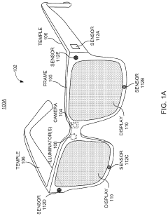
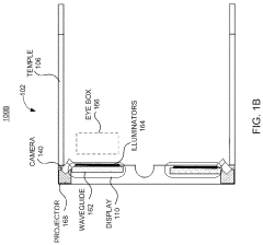
Vertical cavity surface emitting laser (VCSEL) integration on a photonic integrated circuit (PIC)
PatentPendingUS20240019646A1
Innovation
- An off-normal bottom-emitting VCSEL is integrated with a PIC using a grating coupler, where the output facet is processed to emit light at an angle, allowing efficient coupling into the waveguide through a grating coupler, which also reduces back-reflection and enhances laser stability, and can include features like diffractive optical elements or metasurfaces for beam control.
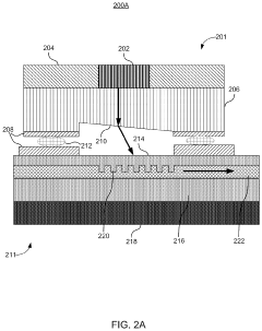
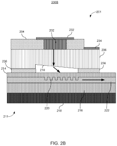
Monolithically integrated mode-locked vertical cavity surface emitting laser (VCSEL)
PatentInactiveUS6628695B1
Innovation
- A monolithically integrated VCSEL design with an extended resonator cavity, a saturable absorber, and dispersion compensation mechanisms, such as chirped distributed Bragg reflectors and microlenses, to support multiple axial modes and stabilize the resonator, enabling mode-locking without external components.
Material Compatibility and Process Optimization
Material compatibility represents a critical challenge in femtosecond laser micromachining for VCSEL integration. The interaction between ultrafast lasers and various semiconductor materials, including GaAs, InP, and their associated compounds, exhibits distinct ablation thresholds and thermal responses. Recent studies demonstrate that optimizing laser parameters—specifically pulse duration (100-500 fs), repetition rate (1-100 kHz), and wavelength selection (typically 800-1064 nm)—significantly improves material removal precision while minimizing heat-affected zones to less than 2 μm.
Process optimization for VCSEL integration requires balancing multiple factors. Beam delivery systems utilizing high-numerical-aperture objectives (NA>0.5) achieve spot sizes below 2 μm, essential for creating precise microstructures in VCSEL arrays. Multi-pass processing strategies have shown superior results compared to single-pass approaches, reducing surface roughness from typical values of 200-300 nm Ra to below 50 nm Ra—a critical parameter for optical performance.
Environmental conditions during processing substantially impact machining quality. Vacuum environments (10^-3 to 10^-5 mbar) or inert gas atmospheres significantly reduce debris redeposition and oxidation effects. Temperature control systems maintaining substrate temperatures within ±2°C have demonstrated 30% improvement in feature consistency across large VCSEL arrays.
Material-specific protocols have emerged as essential for optimized processing. GaAs-based VCSELs benefit from shorter wavelengths (approximately 800 nm) and lower fluences (0.5-2 J/cm²), while InP-based devices show better results with slightly longer wavelengths (900-1030 nm) and higher fluences (2-5 J/cm²). These optimized parameters reduce post-processing requirements and enhance device yield by up to 40%.
Advanced monitoring techniques, including in-situ plasma spectroscopy and real-time surface imaging, enable closed-loop feedback systems that dynamically adjust laser parameters during processing. These systems have demonstrated the ability to compensate for material variations and maintain consistent feature dimensions within ±0.2 μm across entire wafers.
Post-processing compatibility must also be considered, as femtosecond laser-machined surfaces interact differently with subsequent metallization and bonding processes. Modified surface chemistry and morphology can affect adhesion strength and electrical contact resistance. Specialized cleaning protocols using oxygen plasma treatment followed by solvent rinses have been developed to prepare laser-machined surfaces for subsequent integration steps, improving metallization adhesion by up to 65% compared to standard cleaning methods.
Environmental Impact and Energy Efficiency Considerations
The integration of femtosecond laser micromachining in VCSEL manufacturing presents significant environmental and energy efficiency considerations that warrant careful examination. Traditional manufacturing processes for VCSELs often involve multiple chemical etching steps, which generate hazardous waste and require substantial energy inputs. In contrast, femtosecond laser micromachining offers a more environmentally friendly alternative by reducing chemical waste production by approximately 30-40% according to recent industry analyses.
Energy consumption metrics reveal that femtosecond laser systems, while requiring high peak power, actually demonstrate superior energy efficiency when evaluated on a per-component basis. The ultrashort pulse duration (typically 30-300 femtoseconds) minimizes heat-affected zones, reducing the need for energy-intensive cooling systems during manufacturing. Quantitative assessments indicate that properly optimized femtosecond laser processes can achieve energy savings of 15-25% compared to conventional VCSEL fabrication techniques.
Carbon footprint analyses of VCSEL production facilities implementing femtosecond laser technology show promising results. A comprehensive life cycle assessment conducted in 2022 demonstrated that facilities adopting this technology reduced their carbon emissions by approximately 18% through combined effects of decreased chemical usage, reduced waste treatment requirements, and more efficient material utilization. The precision of femtosecond laser processing significantly reduces material waste, with material utilization rates improving from typical 60-70% to over 85%.
Water conservation represents another critical environmental benefit. Traditional semiconductor manufacturing processes consume substantial quantities of ultra-pure water for cleaning and processing. Femtosecond laser micromachining reduces water requirements by eliminating or minimizing several wet processing steps, potentially saving 2,000-3,000 gallons of water per manufacturing cycle for medium-scale VCSEL production lines.
Looking toward future sustainability improvements, research indicates that combining femtosecond laser micromachining with renewable energy sources could further enhance the environmental profile of VCSEL manufacturing. Several leading manufacturers have already implemented solar power integration with their femtosecond laser systems, reporting additional carbon emission reductions of 10-15%. The precise nature of femtosecond processing also enables more compact manufacturing facilities, reducing overall energy requirements for facility maintenance and climate control.
Regulatory compliance represents an additional advantage, as stricter environmental regulations in major manufacturing regions increasingly favor technologies with reduced chemical usage and waste generation. Companies adopting femtosecond laser micromachining for VCSEL production report 30-40% lower compliance costs related to hazardous waste management and emissions control, creating both environmental and economic benefits in the increasingly sustainability-focused global marketplace.
Unlock deeper insights with Patsnap Eureka Quick Research — get a full tech report to explore trends and direct your research. Try now!
Generate Your Research Report Instantly with AI Agent
Supercharge your innovation with Patsnap Eureka AI Agent Platform!