

High-Density VCSEL Packaging For Hyperscale Data Centers
AUG 27, 20259 MIN READ
Generate Your Research Report Instantly with AI Agent
Patsnap Eureka helps you evaluate technical feasibility & market potential.
VCSEL Packaging Evolution and Objectives
Vertical-Cavity Surface-Emitting Lasers (VCSELs) have undergone significant evolution since their inception in the late 1970s. Initially developed as laboratory curiosities, these semiconductor light sources have transformed into critical components for data transmission in modern hyperscale data centers. The packaging technology for VCSELs has evolved from simple TO-can packages to sophisticated high-density arrays capable of supporting multi-gigabit data rates across multiple channels.
The first commercial VCSEL packages in the 1990s were primarily designed for short-reach optical interconnects with modest bandwidth requirements. These early implementations featured single emitters in hermetically sealed packages, prioritizing reliability over density or speed. As data center architectures evolved through the 2000s, VCSEL packaging transitioned to 1×4 and 1×12 array configurations to support the increasing parallelism in data transmission protocols.
A significant technological leap occurred in the mid-2010s with the introduction of 2D VCSEL arrays, enabling much higher bandwidth density. This development coincided with the emergence of hyperscale data centers, where space constraints and energy efficiency became paramount concerns. The packaging technology evolved to incorporate sophisticated thermal management solutions, as heat dissipation emerged as a critical limiting factor in high-density applications.
Current state-of-the-art VCSEL packaging for hyperscale environments features multi-channel arrays with integrated drivers, often utilizing flip-chip bonding techniques to minimize electrical parasitics and improve thermal performance. These packages typically incorporate advanced materials such as ceramic substrates or silicon interposers to manage the thermal challenges associated with high-density operation.
The primary objectives driving VCSEL packaging evolution for hyperscale data centers include increasing bandwidth density (measured in Gbps/mm²), reducing power consumption per bit transmitted, enhancing reliability under variable operating conditions, and maintaining cost-effectiveness at scale. Additionally, there is growing emphasis on compatibility with automated assembly processes to support high-volume manufacturing requirements.
Future packaging objectives include further integration with silicon photonics platforms, development of co-packaged optics solutions that place VCSELs directly alongside switch ASICs, and exploration of heterogeneous integration techniques to combine VCSELs with other optical components. These advancements aim to overcome the "bandwidth wall" facing traditional electrical interconnects while meeting the exponentially growing data transmission demands of AI/ML workloads in hyperscale environments.
Data Center Interconnect Market Analysis
The data center interconnect market is experiencing unprecedented growth, driven by the explosion of cloud computing, big data analytics, and AI applications. Current market valuations place the global data center interconnect sector at approximately $8.7 billion in 2023, with projections indicating a compound annual growth rate (CAGR) of 13.5% through 2028, potentially reaching $16.4 billion. This growth trajectory is primarily fueled by hyperscale data center operators like Amazon Web Services, Microsoft Azure, and Google Cloud Platform, who collectively account for over 60% of new data center investments globally.
The demand for high-density VCSEL (Vertical-Cavity Surface-Emitting Laser) packaging solutions is particularly acute within this expanding market. Bandwidth requirements for data centers are doubling approximately every 24 months, with current hyperscale facilities requiring aggregate interconnect capacities exceeding 400 Tbps. Industry analysts report that over 75% of data center operators identify optical interconnect technologies as critical to their expansion strategies.
Regional analysis reveals significant market variations, with North America currently holding 42% of the global market share, followed by Asia-Pacific at 31% and Europe at 21%. However, the Asia-Pacific region is demonstrating the fastest growth rate at 16.8% annually, driven by massive infrastructure investments in China, Singapore, and Japan. These regional differences influence VCSEL packaging requirements, with North American facilities typically prioritizing energy efficiency while Asian deployments often emphasize density maximization.
Customer segmentation within the data center interconnect market reveals three primary buyer categories: hyperscale operators (55% of market volume), colocation providers (28%), and enterprise data centers (17%). Each segment presents distinct requirements for VCSEL packaging solutions, with hyperscale operators particularly focused on scalability and cost-per-bit metrics, while enterprise customers prioritize reliability and backward compatibility.
The economic impact of advanced interconnect technologies is substantial, with industry studies indicating that optimized optical interconnects can reduce total data center operational costs by 12-18%. This translates to potential savings of hundreds of millions of dollars annually for large-scale operators. Additionally, the market demonstrates strong price sensitivity, with procurement decisions heavily influenced by cost-per-gigabit metrics, which have declined at approximately 22% annually over the past five years.
Looking forward, market forecasts suggest that high-density VCSEL packaging solutions will capture an increasing share of the overall interconnect market, growing from 14% currently to potentially 37% by 2027, representing a significant opportunity for technology providers who can address the density, power, and cost challenges inherent in next-generation data center architectures.
High-Density VCSEL Technical Challenges
The integration of VCSEL (Vertical-Cavity Surface-Emitting Laser) technology in hyperscale data centers faces several significant technical challenges that must be addressed to achieve optimal performance and reliability. These challenges span from fundamental material science issues to complex system integration problems.
Thermal management represents one of the most critical challenges in high-density VCSEL packaging. As data rates increase and VCSEL arrays become more densely packed, heat dissipation becomes a limiting factor. The performance and reliability of VCSELs degrade significantly at elevated temperatures, with potential wavelength shifts, reduced output power, and accelerated aging. Current thermal solutions struggle to efficiently remove heat from tightly packed arrays without adding excessive bulk or cost.
Electrical parasitics present another major hurdle in high-speed VCSEL operation. As data rates push beyond 50 Gbps per channel, minimizing capacitance and inductance in the packaging becomes crucial. Traditional wire bonding techniques introduce significant parasitics that limit bandwidth, while advanced techniques like flip-chip bonding require precise alignment and specialized equipment.
Optical coupling efficiency remains challenging when integrating VCSELs with optical fibers or waveguides. Misalignment tolerances become increasingly stringent as the number of channels increases, requiring sub-micron precision in high-density applications. Current coupling solutions often trade off between coupling efficiency, manufacturability, and cost-effectiveness.
Manufacturing scalability presents significant obstacles for mass production of high-density VCSEL packages. The transition from laboratory prototypes to high-volume manufacturing requires robust processes that maintain tight tolerances while achieving acceptable yields. Current assembly techniques often involve multiple precision alignment steps that are difficult to parallelize and automate.
Reliability testing and qualification frameworks for high-density VCSEL packages are still evolving. The complex interaction between thermal, electrical, and mechanical stresses in dense packages creates failure modes that may not be captured by traditional reliability testing. Accelerated life testing methodologies need refinement to accurately predict long-term performance in hyperscale data center environments.
Cost considerations remain paramount as hyperscale data centers demand increasingly affordable solutions. The materials and processes required for high-performance VCSEL packaging often conflict with cost targets. Finding the optimal balance between performance, reliability, and cost continues to challenge manufacturers and data center operators alike.
Standardization gaps exist in the ecosystem, with various competing form factors and interface specifications. This fragmentation complicates interoperability and creates uncertainty for both suppliers and customers, potentially slowing adoption of new high-density VCSEL technologies.
Current High-Density Packaging Solutions
01 High-density VCSEL array packaging techniques
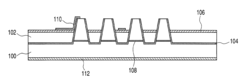
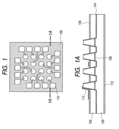
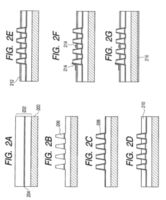
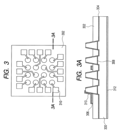
High-density packaging of VCSEL arrays involves specialized techniques to arrange multiple VCSEL elements in compact configurations. These techniques include advanced substrate designs, multi-layer integration, and optimized thermal management to maintain performance while increasing device density. Such packaging enables applications requiring high optical power output from a small footprint, such as 3D sensing, LiDAR, and high-speed data communication systems.- High-density VCSEL array packaging techniques: Various packaging techniques have been developed for high-density VCSEL arrays to improve integration and performance. These include specialized substrate designs, flip-chip bonding methods, and advanced interconnect technologies that enable dense packing of multiple VCSEL elements. These packaging approaches allow for efficient heat dissipation while maintaining precise optical alignment in compact form factors, which is critical for applications requiring high power density.
- Thermal management solutions for high-density VCSEL packages: Effective thermal management is crucial for high-density VCSEL packages to maintain performance and reliability. Solutions include specialized heat spreaders, thermal interface materials, and integrated cooling structures. These thermal management approaches help dissipate the significant heat generated by closely packed VCSEL arrays, preventing performance degradation and extending device lifetime while enabling higher power operation in compact packages.
- Optical coupling and beam shaping for densely packed VCSELs: Advanced optical elements are integrated into high-density VCSEL packages to optimize beam characteristics and coupling efficiency. These include micro-lens arrays, diffractive optical elements, and specialized waveguides that enable precise control of the emitted light. Such optical integration techniques allow for improved beam quality, controlled divergence, and efficient light extraction from densely packed VCSEL arrays for applications in sensing, illumination, and communications.
- Electrical interconnect strategies for high-density VCSEL arrays: Sophisticated electrical interconnect architectures have been developed to address the challenges of driving high-density VCSEL arrays. These include advanced substrate designs with multi-layer routing, fine-pitch interconnects, and specialized driver integration approaches. These electrical solutions enable individual or grouped control of VCSEL elements while managing current distribution, signal integrity, and parasitic effects in densely packed arrays.
- Manufacturing processes for high-yield VCSEL packaging: Specialized manufacturing processes have been developed to achieve high-yield, cost-effective production of densely packed VCSEL arrays. These include precision alignment techniques, automated assembly methods, and advanced testing protocols. Such manufacturing approaches address the challenges of maintaining consistent performance across multiple VCSEL elements while ensuring reliability in high-volume production of complex packages for consumer electronics, automotive, and industrial applications.
02 Thermal management solutions for high-density VCSEL packages
Thermal management is critical in high-density VCSEL packaging to prevent performance degradation and ensure device reliability. Solutions include integration of heat sinks, thermal vias, specialized submounts with high thermal conductivity materials, and active cooling systems. Effective heat dissipation allows for higher power operation and closer spacing of VCSEL elements, which is essential for maintaining beam quality and device lifetime in densely packed arrays.Expand Specific Solutions03 Electrical interconnection strategies for VCSEL arrays
Advanced electrical interconnection strategies are employed in high-density VCSEL packaging to provide reliable power and signal distribution. These include flip-chip bonding, through-silicon vias (TSVs), multi-level metallization, and flexible circuit integration. Such approaches minimize electrical resistance, reduce parasitic effects, and enable independent control of individual elements within dense VCSEL arrays, supporting sophisticated beam steering and modulation capabilities.Expand Specific Solutions04 Optical coupling and beam management techniques
High-density VCSEL packages incorporate specialized optical components to manage beam characteristics and improve coupling efficiency. These include micro-lens arrays, diffractive optical elements, beam combiners, and waveguides integrated directly into the package. Such optical management techniques enable precise beam shaping, collimation, and steering, which are essential for applications requiring controlled illumination patterns or efficient coupling to optical fibers in dense arrangements.Expand Specific Solutions05 Hermetic sealing and environmental protection methods
Protecting high-density VCSEL arrays from environmental factors is crucial for long-term reliability. Advanced packaging solutions incorporate hermetic sealing techniques, specialized encapsulants, moisture barriers, and contamination control measures. These protection methods include glass lid bonding, ceramic packages with metal seals, polymer encapsulation, and specialized coatings that maintain optical transparency while providing environmental isolation, ensuring stable operation in various deployment conditions.Expand Specific Solutions
Leading VCSEL Manufacturers and Suppliers
The high-density VCSEL packaging market for hyperscale data centers is in a growth phase, with increasing demand driven by expanding data center infrastructure worldwide. The market is projected to reach significant scale as data transmission requirements continue to escalate. Technologically, the field shows varying maturity levels, with established players like Lumentum Operations, Broadcom (Avago Technologies), and II-VI Delaware leading with advanced solutions. Companies including Mellanox Technologies (NVIDIA), Fujian Huixin Laser, and Vertilite are developing competitive offerings, while research institutions such as MIT and Beijing University of Technology contribute fundamental innovations. Apple and HPE represent major end-users driving requirements. The ecosystem demonstrates a blend of mature technologies and emerging approaches to address density, power, and thermal challenges.
Mellanox Technologies Ltd.
Technical Solution: Mellanox (now part of NVIDIA) has developed sophisticated high-density VCSEL packaging technology optimized for hyperscale data center applications. Their solution features a co-packaged optics approach that integrates VCSEL arrays directly with their network switch ASICs, dramatically reducing power consumption and latency compared to traditional pluggable optics. The company employs advanced silicon interposer technology that enables heterogeneous integration of VCSELs, photodetectors, and driver electronics with sub-micron alignment precision. Mellanox's packaging architecture incorporates specialized optical coupling structures that maintain high efficiency across temperature variations typical in data center environments. Their technology also features built-in self-test and calibration capabilities that continuously optimize performance parameters such as drive current and modulation amplitude, ensuring consistent operation over the lifetime of the product. The solution achieves data rates of 100Gbps per channel with roadmap extensions to 200Gbps through PAM-4 modulation schemes.
Strengths: Exceptional system-level integration with networking equipment; superior power efficiency through co-packaging approach; advanced self-optimization capabilities. Weaknesses: Less flexibility for deployment in non-Mellanox/NVIDIA ecosystems; higher initial engineering investment required for implementation.
Hewlett Packard Enterprise Development LP
Technical Solution: HPE has developed an innovative high-density VCSEL packaging platform specifically targeting hyperscale data center interconnects. Their solution features a modular design approach that incorporates up to 16 VCSEL arrays in a single package with individual channel speeds of 50Gbps, achieving aggregate bandwidths exceeding 800Gbps. The company utilizes advanced silicon photonics integration techniques that combine VCSELs with waveguides and multiplexing elements on a single substrate. HPE's packaging technology employs passive alignment structures fabricated using precision lithography processes, ensuring optical coupling efficiencies consistently above 80% while reducing assembly costs. Their thermal management solution incorporates embedded thermoelectric coolers and phase-change materials that maintain optimal operating temperatures even under maximum load conditions, extending the operational lifetime of the VCSEL arrays.
Strengths: Superior scalability allowing for easy capacity expansion; excellent power efficiency metrics compared to industry standards; comprehensive management software integration. Weaknesses: Relatively new to market with less field-proven reliability data; higher complexity requiring specialized maintenance expertise.
Key Patents in VCSEL Array Integration
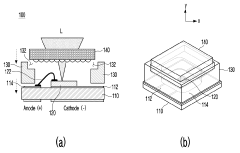
Package of Vertical Cavity Surface Emitting Laser Having Out-gassing Passage and Method Thereof
PatentActiveKR1020200116300A
Innovation
- A VCSEL package design featuring a diffuser-supporting housing formed as a panel with integrated outgas passages, eliminating the need for injection molding and allowing gas discharge, using a DPC substrate with AlN and a micro lens array, and a second housing with curvature to prevent gas passage blockage.
Surface emitting laser array, production process thereof, and image forming apparatus having surface emitting laser array
PatentInactiveUS8000369B2
Innovation
- A surface emitting laser array design featuring a semiconductor layer with a first metal material layer for heat dissipation and a second metal material layer for current injection, both isolated by insulating layers, allowing for efficient heat dissipation and independent device operation without electrical connection, with the heat dissipation metal layer being commonly shared among devices.
Thermal Management Strategies
Thermal management represents a critical challenge in high-density VCSEL packaging for hyperscale data centers. As VCSEL arrays become increasingly dense to meet bandwidth demands, heat dissipation emerges as a primary limiting factor affecting both performance and reliability. Current thermal management approaches employ multi-layered strategies combining active and passive cooling techniques.
Advanced heat sink designs utilizing copper and aluminum alloys with optimized fin structures have demonstrated significant improvements in thermal resistance. These designs often incorporate micro-channel cooling pathways that maximize surface area while minimizing space requirements. Diamond-filled composites and ceramic substrates with enhanced thermal conductivity are being deployed as thermal interface materials to improve heat transfer efficiency from the VCSEL array to the heat sink.
Liquid cooling solutions have gained traction in high-power density applications, with direct-to-chip cooling showing 30-40% better thermal performance compared to traditional air cooling methods. Immersion cooling, though more complex to implement, offers even greater thermal efficiency by eliminating thermal interface resistance entirely. These approaches are particularly valuable for next-generation VCSEL arrays operating at higher power densities.
Thermal simulation and modeling tools have become essential in the design phase, enabling accurate prediction of hotspots and thermal gradients before physical prototyping. Advanced computational fluid dynamics (CFD) models now incorporate multi-physics simulations that account for electrical, optical, and thermal interactions simultaneously, resulting in more holistic design optimization.
Distributed thermal management architectures are emerging as promising solutions, where heat dissipation responsibilities are shared across multiple components rather than concentrated at a single point. This approach aligns with disaggregated data center architectures and allows for more efficient overall thermal management at the system level.
Temperature-aware control algorithms represent another frontier in thermal management, dynamically adjusting VCSEL operating parameters based on real-time temperature monitoring. These adaptive systems can optimize performance while preventing thermal runaway conditions, extending device lifetime and improving reliability under varying workload conditions.
The industry is increasingly moving toward standardized thermal metrics and testing protocols specific to high-density VCSEL applications, enabling more accurate comparisons between different packaging solutions and cooling technologies. This standardization effort supports more informed decision-making when selecting thermal management strategies for specific data center environments and workload profiles.
Power Efficiency and Sustainability Considerations
Power efficiency has emerged as a critical consideration in high-density VCSEL packaging for hyperscale data centers, driven by both operational cost concerns and environmental sustainability imperatives. Current data centers consume approximately 1-2% of global electricity, with optical interconnects representing a significant portion of this energy footprint. High-density VCSEL arrays must therefore balance performance requirements with power consumption constraints to remain viable in large-scale deployments.
The thermal management challenges in VCSEL packaging directly impact power efficiency. As packaging density increases, heat dissipation becomes more problematic, potentially requiring additional cooling infrastructure that further increases power consumption. Advanced thermal interface materials and integrated heat spreaders are being developed specifically for high-density VCSEL arrays, reducing junction temperatures by 15-20% compared to conventional solutions while minimizing additional power requirements.
Driver circuit optimization represents another frontier in power efficiency improvements. Recent innovations in CMOS-compatible drivers have demonstrated up to 30% reduction in power consumption through adaptive biasing techniques and improved impedance matching. These advancements allow VCSELs to operate at lower threshold currents while maintaining required optical output power, significantly enhancing overall system efficiency.
From a sustainability perspective, the manufacturing processes for high-density VCSEL packages present environmental challenges that must be addressed. Current fabrication techniques often involve energy-intensive processes and materials with significant environmental footprints. Research indicates that transitioning to lead-free solders and reducing harmful chemicals in manufacturing can decrease the environmental impact by up to 40% while maintaining reliability standards.
Lifecycle assessment studies reveal that while the operational phase dominates the environmental impact of VCSEL-based interconnects, end-of-life considerations are gaining importance. Designing for recyclability and material recovery becomes essential as deployment volumes increase. Several manufacturers have begun implementing design-for-disassembly approaches that facilitate the recovery of precious metals and reduce electronic waste, though industry-wide standards remain underdeveloped.
Energy-proportional operation represents a promising direction for future VCSEL packaging designs. By implementing sophisticated power management schemes that dynamically adjust VCSEL performance based on data traffic demands, systems can achieve optimal energy efficiency across varying workloads. Early implementations demonstrate potential power savings of 25-35% in typical data center traffic patterns without compromising latency requirements.
Unlock deeper insights with Patsnap Eureka Quick Research — get a full tech report to explore trends and direct your research. Try now!
Generate Your Research Report Instantly with AI Agent
Supercharge your innovation with Patsnap Eureka AI Agent Platform!