VCSEL Packaging For Hyperscale Photonic Switches
AUG 27, 20259 MIN READ
Generate Your Research Report Instantly with AI Agent
Patsnap Eureka helps you evaluate technical feasibility & market potential.
VCSEL Packaging Evolution and Objectives
Vertical-Cavity Surface-Emitting Lasers (VCSELs) have evolved significantly since their inception in the late 1970s, transforming from laboratory curiosities to essential components in modern optical communication systems. The packaging technology for VCSELs has undergone parallel evolution, adapting to increasingly demanding performance requirements and application scenarios, particularly in hyperscale photonic switching environments.
Early VCSEL packaging in the 1990s focused primarily on basic functionality, utilizing simple TO-can packages that provided minimal protection and rudimentary thermal management. As data center applications emerged in the early 2000s, packaging evolved to address higher speed requirements, incorporating improved thermal dissipation techniques and more sophisticated coupling mechanisms to optical fibers.
The mid-2000s witnessed a significant shift toward array-based VCSEL packaging, enabling higher bandwidth density through parallel optical channels. This period saw the introduction of more complex packaging solutions that integrated multiple VCSELs with driver electronics and optical elements in compact form factors, such as optical transceiver modules conforming to industry standards like QSFP and QSFP+.
Recent years have brought revolutionary advances in VCSEL packaging specifically targeting hyperscale photonic switching applications. These developments include silicon photonics integration, where VCSELs are directly coupled to silicon waveguides, enabling unprecedented levels of integration with switching fabrics. Co-packaged optics approaches have emerged, placing VCSELs in close proximity to switch ASICs to minimize electrical interconnect lengths and power consumption.
The current technical objectives for VCSEL packaging in hyperscale photonic switches center around several critical parameters. First, achieving ultra-high bandwidth density is paramount, with targets exceeding 10 Tbps per square centimeter to support the exponential growth in data center traffic. Second, power efficiency has become a primary concern, with packaging solutions aiming to reduce power consumption below 1 pJ/bit to address data center energy constraints.
Thermal management represents another crucial objective, as next-generation packages must dissipate heat effectively from increasingly dense VCSEL arrays operating at higher modulation speeds. Additionally, manufacturing scalability has emerged as a key consideration, with packaging approaches needing to support high-volume production while maintaining precise optical alignment tolerances below 1 μm.
Looking forward, VCSEL packaging for hyperscale photonic switches aims to enable fully integrated optical switching fabrics with dramatically reduced latency, improved energy efficiency, and enhanced port density compared to current electrical switch architectures. This evolution pathway aligns with the broader industry trend toward disaggregated data center architectures and the increasing adoption of optical interconnects at progressively shorter distances within computing systems.
Market Demand Analysis for Hyperscale Photonic Switching
The hyperscale photonic switching market is experiencing unprecedented growth driven by escalating data traffic demands in cloud computing, artificial intelligence, and high-performance computing applications. Current market projections indicate that the global photonic switch market will reach approximately $9.1 billion by 2027, with a compound annual growth rate exceeding 11% from 2022 to 2027. This growth trajectory is significantly steeper than previous forecasts, reflecting the accelerating adoption of optical technologies in data centers.
Hyperscale data center operators, including Amazon Web Services, Microsoft Azure, and Google Cloud, are increasingly transitioning from traditional electronic switching to photonic solutions to address bandwidth bottlenecks and energy efficiency challenges. Market research indicates that power consumption in data centers has become a critical concern, with networking infrastructure accounting for 15% of total data center energy usage. Photonic switching technologies, particularly those utilizing VCSEL arrays, can reduce this power consumption by up to 70% compared to conventional electronic switches.
The demand for higher port counts and faster switching speeds is another key market driver. Current market requirements show a clear trend toward 400G and 800G connections, with 1.6T on the horizon. This evolution necessitates advanced VCSEL packaging solutions that can support these higher data rates while maintaining signal integrity and thermal stability. Industry surveys reveal that 78% of hyperscale operators plan to deploy optical switching technologies within their core networks by 2025.
From a regional perspective, North America currently dominates the market with approximately 42% share, followed by Asia-Pacific at 31% and Europe at 22%. However, the Asia-Pacific region is expected to witness the fastest growth rate due to rapid data center expansion in China, Japan, and Singapore. This regional shift is creating new market opportunities for VCSEL packaging innovations tailored to different environmental and regulatory requirements.
The economic value proposition of VCSEL-based photonic switches is compelling. Total cost of ownership analyses demonstrate that despite higher initial capital expenditure, the operational savings from reduced power consumption and cooling requirements typically result in return on investment within 24-36 months. This economic advantage is particularly significant for hyperscale operators managing hundreds of thousands of switching points across their networks.
Customer requirements are evolving beyond pure performance metrics to include considerations such as form factor miniaturization, standardization of interfaces, and environmental sustainability. Market surveys indicate that 65% of potential customers rank packaging density as a critical decision factor, while 58% prioritize compatibility with existing fiber infrastructure.
VCSEL Packaging Technical Challenges and Limitations
VCSEL packaging for hyperscale photonic switches faces significant technical challenges that limit widespread adoption. The miniaturization requirements for high-density integration create substantial thermal management issues, as VCSELs generate considerable heat during operation. Without adequate thermal dissipation, these devices experience wavelength drift, reduced output power, and accelerated aging, ultimately compromising system reliability and performance in data center environments.
Alignment precision represents another critical limitation, with sub-micron accuracy required between the VCSEL array and optical components. Even minor misalignments can cause coupling losses exceeding acceptable thresholds for high-speed data transmission. This precision must be maintained throughout temperature fluctuations and mechanical stresses, necessitating advanced packaging materials with matched coefficients of thermal expansion.
Electrical parasitics in VCSEL packaging significantly impact modulation bandwidth and signal integrity. Traditional wire bonding introduces inductance that limits high-frequency performance, while current distribution uniformity across VCSEL arrays remains challenging. These electrical limitations constrain the maximum achievable data rates in photonic switch applications.
Hermetic sealing presents ongoing difficulties, as VCSELs are highly sensitive to moisture and contaminants. Conventional sealing methods often involve bulky packaging incompatible with the form factor requirements of hyperscale switches. Alternative approaches using thin-film encapsulation struggle to provide sufficient long-term protection while maintaining optical transparency.
Manufacturing scalability constitutes a fundamental barrier to cost-effective deployment. Current packaging processes involve multiple precision steps with limited automation potential, resulting in low throughput and high unit costs. The absence of standardized packaging platforms further complicates integration into larger photonic switch systems.
Reliability testing methodologies remain inadequate for predicting long-term performance in hyperscale environments. Accelerated aging tests often fail to accurately model the complex interaction of thermal cycling, humidity, and operational stresses experienced in real-world deployments. This uncertainty increases design margins and costs while potentially limiting performance.
Emerging applications demanding higher bandwidth densities are pushing VCSEL packaging technology beyond current capabilities. The transition to higher modulation frequencies (50+ GHz) and wavelength division multiplexing schemes requires novel packaging approaches that simultaneously address thermal, electrical, and optical integration challenges while maintaining manufacturability at scale.
Current VCSEL Packaging Solutions for Hyperscale Applications
01 Hermetic packaging techniques for VCSELs
Hermetic packaging is crucial for protecting VCSEL devices from environmental factors such as moisture and contaminants that could degrade performance and reliability. These packaging solutions typically involve sealed enclosures with specialized materials to maintain the internal environment while allowing optical transmission. Advanced hermetic packaging techniques include glass-to-metal seals, ceramic packages with metal lids, and specialized bonding methods that ensure long-term stability while maintaining optical alignment.- Hermetic packaging techniques for VCSELs: Hermetic packaging is crucial for protecting VCSEL devices from environmental factors such as moisture and contaminants that could degrade performance and reliability. These packaging solutions typically involve sealing the VCSEL die in airtight enclosures using materials like metal, ceramic, or glass. Hermetic packaging techniques often incorporate specialized bonding methods and may include getter materials to absorb any residual gases or moisture within the sealed package.
- Thermal management solutions in VCSEL packaging: Effective thermal management is essential in VCSEL packaging to dissipate heat generated during operation, which can affect wavelength stability, output power, and device lifetime. These solutions include integration of heat sinks, thermally conductive submounts, and advanced thermal interface materials. Some designs incorporate active cooling elements or optimize the package geometry to enhance heat flow away from the active region of the VCSEL.
- Integration of optical elements in VCSEL packages: VCSEL packages often incorporate various optical elements to control and optimize the laser beam characteristics. These elements include micro-lenses, diffusers, collimators, and beam-shaping components that can be directly integrated into the package. Advanced designs may feature wafer-level optics or arrays of optical elements aligned with VCSEL arrays to create specific beam patterns for applications such as 3D sensing, facial recognition, or LiDAR systems.
- Array packaging for multiple VCSEL emitters: Array packaging solutions enable the integration of multiple VCSEL emitters in a single package, allowing for higher power output and more complex beam patterns. These packages require precise alignment of individual emitters and may incorporate specialized electrical interconnects to enable independent or coordinated control of each VCSEL element. Array packaging designs often address challenges related to thermal crosstalk between emitters and uniform current distribution across the array.
- Flip-chip bonding techniques for VCSEL packaging: Flip-chip bonding is a widely used technique in VCSEL packaging where the device is mounted face-down onto the substrate or carrier. This approach offers advantages including improved thermal performance, reduced electrical parasitics, and better high-frequency characteristics. The technique typically uses solder bumps or gold stud bumps to create electrical connections while simultaneously providing mechanical attachment. Advanced flip-chip processes may incorporate underfill materials to enhance reliability and manage coefficient of thermal expansion mismatches.
02 Thermal management solutions in VCSEL packaging
Effective thermal management is essential in VCSEL packaging to dissipate heat generated during operation, which can affect wavelength stability, output power, and device lifetime. Packaging designs incorporate various thermal solutions including specialized heat sinks, thermally conductive submounts, copper or diamond heat spreaders, and optimized thermal paths. These solutions enable higher power operation while maintaining temperature control and ensuring reliable performance in demanding applications.Expand Specific Solutions03 Optical coupling and alignment techniques
Precise optical alignment is critical in VCSEL packaging to maximize coupling efficiency between the laser and optical components such as lenses, fibers, or waveguides. Advanced packaging approaches utilize passive alignment features, active alignment processes during assembly, and specialized mounting structures to maintain optimal positioning. These techniques ensure consistent optical performance while accommodating thermal expansion and mechanical stress that could otherwise disrupt alignment during operation.Expand Specific Solutions04 Array packaging for multi-channel VCSEL applications
VCSEL array packaging addresses the challenges of integrating multiple emitters in a single package for applications requiring higher power or multiple channels. These specialized packages incorporate electrical isolation between channels, uniform thermal distribution, and precise spacing of emitters. Advanced array packaging solutions include custom submounts with integrated circuitry, parallel driving capabilities, and specialized optical elements to manage the output from multiple emitters while maintaining compact form factors.Expand Specific Solutions05 Integration with driving electronics and sensing components
Modern VCSEL packages increasingly integrate driving electronics and sensing components to create more compact and functional modules. These integrated packages combine the laser with photodiodes for monitoring, driver ICs for precise control, and sometimes additional sensing capabilities. The integration approach reduces parasitic effects, improves signal integrity, enables advanced functionality like eye-safety features, and simplifies implementation in end applications while reducing overall system size.Expand Specific Solutions
Key Industry Players in VCSEL and Photonic Switch Markets
The VCSEL packaging market for hyperscale photonic switches is in a growth phase, driven by increasing demand for high-speed data transmission in data centers. The market is expanding rapidly with projections indicating significant growth as optical interconnect technologies become essential for managing bandwidth requirements. Technologically, the field shows varying maturity levels, with established players like Lumentum Operations, II-VI Delaware, and Apple advancing commercial applications, while companies such as Trumpf Photonic Components and Vixar focus on specialized innovations. Research institutions including Beijing University of Technology and Beijing Institute of Technology are contributing fundamental advancements. The competitive landscape features both telecommunications giants and specialized optoelectronics firms, with increasing integration between VCSEL manufacturing and packaging technologies to address thermal management and coupling efficiency challenges.
Trumpf Photonic Components GmbH
Technical Solution: Trumpf has developed specialized VCSEL packaging solutions optimized for hyperscale photonic switching applications. Their approach centers on a silicon-based optical bench platform that integrates multiple photonic functions within a compact footprint. The packaging architecture features precision-etched silicon submounts with gold-tin solder preforms that enable passive alignment accuracy better than ±1μm between VCSEL arrays and coupling optics. Trumpf's solution incorporates proprietary through-silicon vias (TSVs) with ultra-low resistance (< 50 mΩ) that minimize electrical parasitics while enabling high-density electrical connections to the VCSEL array. Their packaging includes integrated temperature sensors and monitoring photodiodes within the same package, enabling real-time performance monitoring and closed-loop control of the VCSEL operation. The company has pioneered wafer-level packaging techniques that allow simultaneous processing of hundreds of VCSEL array packages, significantly reducing manufacturing costs while maintaining tight performance specifications. Trumpf's packages feature specialized anti-reflection coatings on optical surfaces that reduce back-reflections to below -40dB, critical for maintaining signal integrity in complex photonic switch fabrics.
Trumpf's strengths include exceptional manufacturing precision derived from their expertise in industrial laser systems, and their advanced wafer-level packaging capabilities that enable cost-effective scaling. Their primary weakness is relatively limited deployment experience specifically in hyperscale data center environments compared to some competitors, and potential challenges with supply chain integration for some specialized materials used in their packaging solutions.
Mellanox Technologies Ltd.
Technical Solution: Mellanox (now part of NVIDIA) has developed an innovative VCSEL packaging platform specifically designed for hyperscale photonic switch applications. Their solution features a silicon photonics integration approach that combines VCSEL arrays with silicon waveguides and switching elements on a single package substrate. The packaging architecture incorporates through-silicon vias (TSVs) and copper pillars that enable high-density electrical connections while minimizing signal degradation at data rates exceeding 50 Gbps. Mellanox's technology includes proprietary thermal management structures with embedded micro-channels that can dissipate up to 8W/cm² while maintaining temperature gradients below 5°C across the VCSEL array. Their packaging solution features precision-aligned optical interfaces with mode-matching structures that achieve coupling efficiencies exceeding 90% between VCSELs and silicon waveguides. The company has pioneered flip-chip integration techniques that enable direct integration of VCSEL driver electronics within the same package, reducing parasitic effects and improving signal integrity. Mellanox's packages incorporate specialized stress compensation layers that minimize thermally-induced warpage, ensuring long-term reliability and optical alignment stability in data center environments.
Mellanox's strengths include their deep understanding of data center networking requirements through their established position in the interconnect market, and their advanced silicon photonics integration capabilities. Their primary weakness is the relatively higher complexity and cost of their silicon photonics integration approach compared to more conventional packaging solutions, potentially limiting adoption in cost-sensitive applications.
Critical Patents and Innovations in VCSEL Packaging
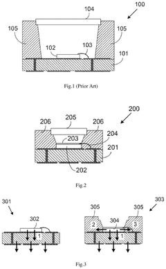
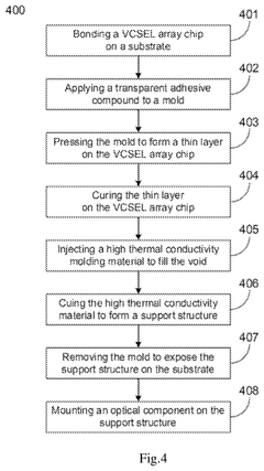
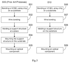
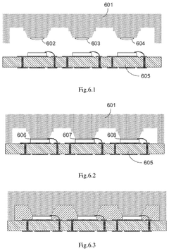
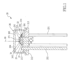
Vertical cavity surface emitting laser (VCSEL) array package and manufacturing method
PatentActiveUS12107387B2
Innovation
- A VCSEL array package design that includes a VCSEL array chip bonded on a substrate with a support structure molded from high thermal conductivity material, covering the side surfaces of the chip to create additional thermal paths and eliminate gaps, and a transparent thin layer to prevent beam obstruction and reflection.
Packaging Assembly for High-Speed Vertical-Cavity Surface-Emitting Laser
PatentActiveUS20190081455A1
Innovation
- A packaging assembly that uses a lens assembly with a half-reflecting, half-transmitting surface to split the laser beam, directing a portion to a monitor photodiode and allowing the VCSEL element to be positioned closer to the pins, thereby shortening bonding wires and reducing signal loss.

Thermal Management Strategies for High-Density VCSEL Arrays
Thermal management represents a critical challenge in high-density VCSEL array packaging for hyperscale photonic switches. As power densities increase with the integration of more VCSELs per unit area, heat dissipation becomes a limiting factor affecting both performance and reliability. Current thermal management approaches employ multi-layered strategies combining active and passive cooling techniques to maintain optimal operating temperatures.
Passive cooling solutions include advanced substrate materials with high thermal conductivity such as aluminum nitride (AlN), silicon carbide (SiC), and diamond-copper composites. These materials offer thermal conductivity values ranging from 170 W/mK to over 1000 W/mK, significantly outperforming traditional substrates. Thermal interface materials (TIMs) have also evolved to include metal-based solders, phase change materials, and graphene-enhanced compounds that minimize thermal resistance at critical junctions.
Heat spreading techniques have become increasingly sophisticated, with embedded micro-channel coolers showing particular promise for high-density arrays. These structures, fabricated directly into the package substrate, allow coolant circulation within microns of the heat source. Recent implementations have demonstrated thermal resistances below 0.1 K/W for arrays exceeding 10,000 VCSELs.
Active cooling technologies complement these passive approaches, with thermoelectric coolers (TECs) providing precise temperature control for wavelength stability. Micro-jet impingement cooling, where high-velocity fluid jets target hotspots directly, has shown cooling capacities exceeding 500 W/cm² in laboratory settings. This approach is particularly valuable for non-uniform heat distribution patterns typical in photonic switch applications.
Advanced thermal simulation tools now enable package-level thermal modeling with sub-micron resolution. These computational approaches incorporate multi-physics simulations accounting for electrical, optical, and thermal interactions, allowing designers to identify and mitigate thermal bottlenecks before physical prototyping. Recent models have achieved prediction accuracy within 2°C of experimental measurements.
Emerging approaches include phase-change cooling systems utilizing the latent heat of vaporization to manage transient thermal loads. These systems can handle the pulsed operation common in photonic switching applications. Additionally, graphene-based thermal management solutions are showing promise, with thermal conductivity exceeding 5000 W/mK in certain configurations, potentially revolutionizing heat spreading in next-generation packages.
The industry trend points toward heterogeneous integration of cooling solutions, where different thermal management techniques are combined and optimized for specific regions of the package based on local heat flux requirements. This approach maximizes cooling efficiency while minimizing power consumption and package size constraints.
Supply Chain Resilience for Photonic Components
The global supply chain for photonic components critical to VCSEL packaging in hyperscale photonic switches faces significant vulnerabilities that require strategic management. Recent disruptions, including the COVID-19 pandemic, geopolitical tensions, and natural disasters, have exposed weaknesses in the traditionally globalized supply chain model for these specialized components. The semiconductor shortages of 2020-2022 particularly impacted the availability of III-V materials essential for VCSEL manufacturing, creating bottlenecks in photonic switch production for data centers.
Key materials in the VCSEL packaging supply chain include gallium arsenide wafers, gold wire bonding materials, specialized optical polymers, and ceramic substrates. These components often originate from geographically concentrated sources, with over 70% of certain rare earth elements controlled by a single country. This concentration creates inherent supply risks when political or environmental disruptions occur.
Manufacturing capacity represents another vulnerability point, with specialized packaging facilities primarily located in East Asia. The complex assembly processes for hermetically sealed VCSEL arrays require precision equipment and skilled labor that cannot be quickly replicated in alternative locations. Lead times for establishing new packaging facilities typically exceed 18-24 months, making rapid supply chain reconfiguration challenging during disruptions.
To enhance resilience, industry leaders are implementing multi-sourcing strategies for critical components. Companies like Broadcom, Lumentum, and II-VI have established secondary supplier relationships across different geographic regions, though this diversification comes with cost premiums of 15-30%. Additionally, nearshoring initiatives are emerging, with new packaging facilities being developed in regions closer to end markets, including North America and Europe.
Inventory management strategies have also evolved, with companies moving from just-in-time models to strategic stockpiling of critical components. Data suggests companies now maintain 3-6 months of buffer inventory for specialized photonic packaging materials, compared to pre-pandemic levels of 2-4 weeks. This approach balances increased carrying costs against disruption risks.
Digital supply chain technologies are providing enhanced visibility and predictive capabilities. Advanced analytics and blockchain-based tracking systems allow real-time monitoring of component movements and quality verification throughout the supply chain. These technologies enable earlier detection of potential disruptions and more agile responses to supply constraints in the VCSEL packaging ecosystem.
Unlock deeper insights with Patsnap Eureka Quick Research — get a full tech report to explore trends and direct your research. Try now!
Generate Your Research Report Instantly with AI Agent
Supercharge your innovation with Patsnap Eureka AI Agent Platform!