Low-Cost Packaging Routes For High-Volume VCSEL Production
AUG 27, 20259 MIN READ
Generate Your Research Report Instantly with AI Agent
Patsnap Eureka helps you evaluate technical feasibility & market potential.
VCSEL Packaging Evolution and Objectives
Vertical-Cavity Surface-Emitting Lasers (VCSELs) have undergone significant evolution since their inception in the late 1970s. Initially developed as laboratory curiosities, these semiconductor light sources have transformed into critical components for various applications including data communications, sensing, and consumer electronics. The packaging technology for VCSELs has evolved in parallel with their increasing commercial importance, transitioning from bulky, expensive hermetic packages to more streamlined and cost-effective solutions.
Early VCSEL packaging (1990s-2000s) primarily utilized TO-can hermetic packages, which provided excellent protection but were costly and limited in terms of integration density. As market demands shifted toward higher volumes and lower costs, particularly with the emergence of mobile device applications, packaging strategies began to evolve toward more economical approaches while maintaining essential performance parameters.
The mid-2000s saw the introduction of ceramic submounts and simplified non-hermetic packaging for less demanding applications. This period marked the beginning of a fundamental shift in VCSEL packaging philosophy, balancing reliability requirements against cost considerations. By the 2010s, wafer-level packaging (WLP) techniques began gaining traction, offering significant cost reductions for high-volume production.
Current objectives in VCSEL packaging center around several key priorities. First is cost reduction, as VCSELs transition from specialized components to mass-market devices used in consumer electronics. The industry aims to achieve packaging costs below $0.10 per device for high-volume applications, representing a significant challenge that requires fundamental innovations in materials and processes.
Second is scalability, with packaging solutions that can support production volumes exceeding hundreds of millions of units annually. This objective necessitates highly automated assembly processes and simplified packaging architectures that minimize handling steps and material costs.
Third is miniaturization, as applications in mobile devices and wearable technology demand increasingly compact form factors. Modern VCSEL packages must achieve footprints below 2×2mm while maintaining optical performance and thermal management capabilities.
Fourth is thermal management, which remains critical as VCSEL arrays increase in power density. Packaging solutions must efficiently dissipate heat to prevent performance degradation and ensure device longevity, particularly in consumer applications where active cooling is not feasible.
Finally, integration capability has become a paramount objective, with packaging approaches that facilitate the combination of VCSELs with photodetectors, driver ICs, and optical elements. This integration trend supports the development of complete sensing modules rather than discrete components, adding value while potentially reducing overall system costs.
Market Demand Analysis for High-Volume VCSEL Applications
The VCSEL (Vertical-Cavity Surface-Emitting Laser) market has experienced significant growth in recent years, primarily driven by increasing adoption in consumer electronics, particularly in 3D sensing applications for facial recognition systems in smartphones. According to industry reports, the global VCSEL market was valued at approximately $2.1 billion in 2020 and is projected to reach $5.3 billion by 2026, representing a compound annual growth rate (CAGR) of 17.3% during the forecast period.
The demand for VCSELs is particularly strong in three key application segments. First, the consumer electronics sector, where Apple's implementation of Face ID technology in iPhones has set a precedent for facial recognition systems, creating substantial demand for VCSEL arrays. This trend is expanding as Android manufacturers increasingly incorporate similar technologies into their devices. Market research indicates that a single high-end smartphone may contain multiple VCSEL chips, with annual smartphone shipments exceeding 1.3 billion units globally.
Second, the automotive industry represents a rapidly growing market for VCSEL technology. Advanced driver-assistance systems (ADAS) and autonomous driving capabilities require sophisticated LiDAR systems, many of which utilize VCSEL arrays. Industry forecasts suggest that the automotive LiDAR market will grow at a CAGR of 28.4% through 2025, creating substantial demand for high-volume, cost-effective VCSEL solutions.
Third, data communications applications continue to drive VCSEL demand. With increasing bandwidth requirements in data centers and the ongoing expansion of 5G infrastructure, VCSELs are essential components in high-speed optical interconnects. The data center market alone is expected to consume over 100 million VCSEL units annually by 2023.
Market analysis reveals a critical price sensitivity across these applications. While early adopters in premium smartphone segments were less price-sensitive, mass market adoption requires significant cost reductions. Industry surveys indicate that packaging costs currently represent 60-70% of total VCSEL module production expenses, making packaging innovation the primary lever for enabling broader market penetration.
The geographical distribution of VCSEL demand shows Asia-Pacific as the fastest-growing region, with China, South Korea, and Taiwan leading manufacturing capacity expansion. North America remains a significant market due to data center infrastructure and defense applications, while European demand is primarily driven by automotive and industrial automation sectors.
Market forecasts indicate that successful development of low-cost packaging solutions could potentially expand the addressable market for VCSELs by 35-40% by enabling adoption in mid-range consumer devices and accelerating implementation in automotive applications where cost constraints have limited deployment.
Current Packaging Technologies and Cost Barriers
The current VCSEL packaging landscape is dominated by several key technologies, each with distinct cost implications for high-volume production. Traditional TO-can packages, while reliable and well-established, involve complex assembly processes requiring precise alignment of optical components and wire bonding, resulting in significant labor costs and slower throughput rates. These packages also utilize gold-plated components and hermetic sealing, further elevating material expenses.
Surface-mount technology (SMT) packages have emerged as an alternative, offering better compatibility with standard PCB assembly processes. However, the specialized materials required for these packages, including ceramic substrates and custom lens arrays, contribute substantially to overall costs. Additionally, the precision alignment requirements during assembly remain a significant cost driver even in automated production lines.
Chip-scale packaging (CSP) represents a more recent advancement, reducing material usage by minimizing package size. Despite this advantage, CSP approaches often require specialized handling equipment and processes due to the delicate nature of the miniaturized components, creating barriers to widespread adoption in cost-sensitive applications.
A major cost barrier across all packaging technologies is thermal management. VCSELs generate significant heat during operation, necessitating effective heat dissipation solutions. Current approaches include integration of thermal interface materials and heat spreaders, which add both material costs and assembly complexity. The trade-off between thermal performance and cost optimization remains a critical challenge.
Testing and quality assurance represent another substantial cost component. Current practices often involve multiple testing stages throughout the packaging process, including die-level testing, post-packaging optical testing, and reliability verification. These steps, while essential for ensuring performance, add significant time and equipment costs to the production flow.
Supply chain considerations further impact packaging economics. Many specialized materials and components used in VCSEL packaging have limited supplier options, creating potential bottlenecks and price vulnerabilities. The geographical distribution of packaging expertise and facilities also affects overall production costs, with significant concentration in East Asia.
Automation levels vary considerably across different packaging approaches. While some processes have achieved high automation, others still rely on semi-manual operations for critical steps like alignment and inspection. This inconsistency in automation capability creates uneven cost structures across the packaging workflow and limits overall throughput potential in high-volume scenarios.
Low-Cost Packaging Solutions Assessment
01 Cost-effective packaging techniques for VCSELs
Various packaging techniques have been developed to reduce the cost of VCSEL manufacturing. These include simplified assembly processes, integration of multiple components in a single package, and automated packaging methods. These techniques aim to minimize material usage, reduce assembly steps, and increase production throughput, thereby lowering the overall packaging cost while maintaining performance requirements.- Cost-effective packaging techniques for VCSELs: Various cost-effective packaging techniques have been developed for VCSELs to reduce manufacturing expenses while maintaining performance. These include simplified assembly processes, automated packaging methods, and the use of standardized components. By optimizing the packaging process, manufacturers can significantly reduce production costs while ensuring reliable operation of VCSEL devices. These techniques often involve innovative substrate materials and integration approaches that minimize the number of components and assembly steps.
- Integration of VCSELs in compact packaging solutions: Compact packaging solutions for VCSELs focus on miniaturization while maintaining thermal management and optical performance. These solutions include chip-scale packaging, wafer-level packaging, and integration with other optical components in small form factors. The compact designs reduce material usage and simplify assembly processes, contributing to overall cost reduction. Advanced integration techniques allow for higher density arrays and improved functionality in smaller packages, which is particularly important for consumer electronics and mobile applications.
- Materials selection for cost-optimized VCSEL packaging: The selection of packaging materials significantly impacts the overall cost of VCSEL devices. Cost-optimized materials include specialized polymers, ceramic substrates, and metal alloys that offer a balance between performance and affordability. These materials are selected based on their thermal conductivity, mechanical stability, and compatibility with automated assembly processes. By replacing expensive traditional packaging materials with more cost-effective alternatives that meet performance requirements, manufacturers can reduce production costs while maintaining device reliability and longevity.
- Mass production techniques for VCSEL packaging: Mass production techniques for VCSEL packaging focus on high-volume manufacturing processes that reduce per-unit costs. These include wafer-level testing, parallel processing, and automated assembly lines specifically designed for optical components. By implementing efficient production workflows and quality control systems, manufacturers can achieve economies of scale that significantly reduce packaging costs. Advanced techniques such as panel-level packaging and batch processing further enhance production efficiency and yield rates for VCSEL devices.
- Thermal management solutions for cost-effective VCSEL packaging: Thermal management is critical for VCSEL performance and reliability, but can significantly impact packaging costs. Cost-effective thermal solutions include innovative heat sink designs, thermally conductive adhesives, and passive cooling structures that maintain operating temperatures without expensive active cooling components. These approaches balance thermal performance with manufacturing complexity to optimize overall device cost. By efficiently managing heat dissipation through package design rather than additional components, manufacturers can reduce both material and assembly costs while ensuring proper device operation.
02 Wafer-level packaging for cost reduction
Wafer-level packaging approaches significantly reduce VCSEL packaging costs by processing multiple devices simultaneously. This method allows for batch processing of hundreds or thousands of devices on a single wafer before separation, eliminating individual device handling. The approach includes wafer-level testing, alignment, bonding, and optical element integration, resulting in substantial cost savings in high-volume production scenarios.Expand Specific Solutions03 Materials selection for cost-optimized VCSEL packaging
The selection of packaging materials plays a crucial role in determining VCSEL packaging costs. Innovations include using lower-cost substrate materials, simplified heat sinks, polymer-based optical components, and alternative bonding materials. These material choices must balance cost reduction with maintaining essential performance characteristics such as thermal management, optical alignment, and long-term reliability.Expand Specific Solutions04 Integration approaches for multi-component VCSEL systems
Integration strategies for VCSEL systems focus on combining multiple components into unified packages to reduce assembly costs. These approaches include integrating VCSELs with photodetectors, driver circuits, and optical elements in single packages. By reducing the number of discrete components and assembly steps, these integration methods significantly lower packaging costs while enabling more compact designs for applications in consumer electronics and sensing systems.Expand Specific Solutions05 Automated assembly and testing for high-volume cost reduction
Automated assembly and testing processes have been developed to reduce VCSEL packaging costs in high-volume production environments. These include machine vision alignment systems, automated die bonding, robotic handling, and parallel testing methodologies. By minimizing human intervention and increasing throughput, these approaches significantly reduce labor costs and improve yield rates, making VCSELs more economically viable for mass-market applications.Expand Specific Solutions
Key Industry Players in VCSEL Manufacturing Ecosystem
The low-cost packaging market for high-volume VCSEL production is currently in a growth phase, with increasing adoption across consumer electronics, automotive LiDAR, and data communications sectors. The global market is expanding rapidly, projected to reach significant scale as applications diversify beyond 3D sensing. Technologically, the field shows varying maturity levels among key players. Companies like Finisar, II-VI (now Coherent), and Lumentum lead with established manufacturing processes, while Chinese firms including Fujian Huixin Laser, Yangzhou Changelight, and Suzhou Everbright Photonics are rapidly advancing their capabilities. Research institutions like the Institute of Semiconductors CAS collaborate with industry to develop innovative packaging solutions that balance cost reduction with performance requirements for next-generation applications.
II-VI Delaware, Inc.
Technical Solution: II-VI has developed advanced wafer-level packaging solutions for VCSEL arrays that significantly reduce manufacturing costs while maintaining high performance. Their approach integrates multiple process steps at the wafer level, including hermetic sealing and optical element integration. The company utilizes automated precision alignment techniques during assembly, achieving sub-micron accuracy while processing hundreds of devices simultaneously. Their proprietary glass frit bonding technology creates reliable hermetic seals at lower temperatures than traditional methods, reducing thermal stress on sensitive components. II-VI has also pioneered the use of through-silicon vias (TSVs) for VCSEL arrays, enabling vertical electrical connections that improve thermal management and reduce package footprint. Their manufacturing facilities implement high-volume semiconductor processing equipment adapted specifically for photonics applications, achieving economies of scale comparable to traditional semiconductor manufacturing[1][3].
Strengths: Industry-leading wafer-level packaging expertise, vertical integration of materials and processes, and established high-volume manufacturing infrastructure. Weaknesses: Higher initial capital investment requirements and potential challenges in adapting to rapidly evolving VCSEL design specifications for emerging applications.
Finisar Corp.
Technical Solution: Finisar has developed a comprehensive low-cost packaging platform for high-volume VCSEL production centered around their patented non-hermetic packaging technology. This approach eliminates expensive hermetic sealing requirements by utilizing specialized polymer materials that provide adequate environmental protection while being compatible with standard surface-mount assembly processes. Their manufacturing process incorporates automated optical alignment systems that achieve passive alignment accuracy below 1μm, significantly reducing assembly time and labor costs. Finisar employs advanced wafer-level testing methodologies that identify defective devices before packaging, improving yield rates by approximately 15%. The company has also pioneered the use of panel-level packaging for VCSELs, processing multiple wafers simultaneously on larger substrates to maximize throughput and reduce per-unit costs. Their facilities utilize modified semiconductor back-end equipment, allowing them to leverage existing high-volume manufacturing infrastructure rather than developing specialized photonics assembly lines[2][4].
Strengths: Non-hermetic packaging expertise reduces material costs, established high-volume manufacturing capabilities, and strong integration with existing electronics supply chains. Weaknesses: Non-hermetic solutions may have reliability limitations in certain harsh environments, and the company faces increasing competition from vertically integrated manufacturers.
Critical Patents and Innovations in VCSEL Packaging
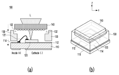
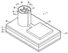
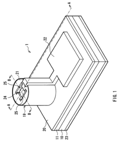
Package of Vertical Cavity Surface Emitting Laser Having Out-gassing Passage and Method Thereof
PatentActiveKR1020200116300A
Innovation
- A VCSEL package design featuring a diffuser-supporting housing formed as a panel with integrated outgas passages, eliminating the need for injection molding and allowing gas discharge, using a DPC substrate with AlN and a micro lens array, and a second housing with curvature to prevent gas passage blockage.
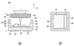
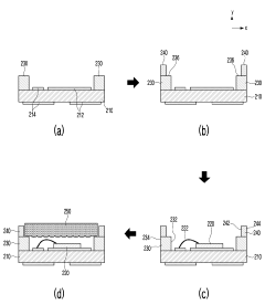
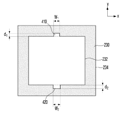
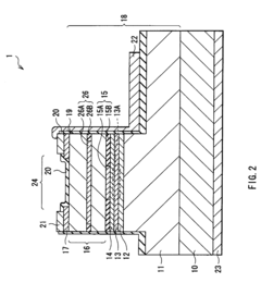
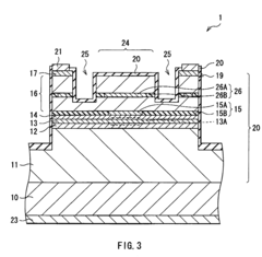
Vertical cavity surface emitting laser and method for manufacturing the same
PatentInactiveUS7675956B2
Innovation
- A VCSEL design featuring a semiconductor lamination structure with grooves and oxidation layers or insulating layers that create tension stress, allowing for polarization component control without requiring special substrates, thereby stabilizing the polarization direction of laser light.
Supply Chain Optimization for VCSEL Production
The optimization of supply chain for VCSEL (Vertical-Cavity Surface-Emitting Laser) production represents a critical factor in achieving cost-effective manufacturing at high volumes. Current VCSEL supply chains often suffer from fragmentation and inefficiencies that significantly impact final product costs. Analysis of existing supply chains reveals that approximately 60-70% of VCSEL production costs stem from packaging and testing processes, presenting substantial opportunities for optimization.
Key suppliers in the VCSEL ecosystem include wafer manufacturers, epitaxial growth specialists, device fabrication facilities, packaging houses, and testing services. The geographical distribution of these suppliers creates logistical challenges, with most epitaxial growth expertise concentrated in North America and Europe, while packaging capabilities are predominantly located in East Asia. This geographical disparity introduces transportation costs, time delays, and potential quality control issues.
Vertical integration strategies have emerged as effective approaches for supply chain optimization. Companies like Lumentum and II-VI have successfully implemented backward integration by acquiring key suppliers, resulting in reported cost reductions of 15-25% and improved production yields. Alternatively, strategic partnerships between specialized entities across the supply chain have demonstrated similar efficiency improvements without the capital requirements of full integration.
Just-in-time inventory management systems specifically adapted for VCSEL production cycles show promise in reducing working capital requirements by up to 30%. These systems must account for the unique characteristics of VCSEL manufacturing, including wafer processing times and testing requirements. Implementation of advanced tracking systems using IoT sensors throughout the supply chain has enabled real-time monitoring of components, reducing delays and improving quality control.
Standardization of packaging interfaces and testing protocols represents another significant opportunity. Industry consortia are working to establish common standards that would enable more interchangeable components and testing equipment, potentially reducing costs by 10-15% through increased competition and economies of scale. Early adopters of these standardization efforts have reported simplified qualification processes and faster time-to-market.
Regional manufacturing hubs that co-locate multiple supply chain elements are emerging as effective models for high-volume production. These hubs minimize transportation costs and enable tighter integration between process steps. Companies implementing this approach have documented cycle time reductions of up to 40% and corresponding improvements in production flexibility to meet variable demand patterns.
Manufacturing Scalability Challenges
The scaling of VCSEL production to high volumes presents significant manufacturing challenges that must be addressed to achieve cost-effective solutions. Current VCSEL packaging processes often rely on traditional semiconductor packaging techniques that were not specifically designed for the unique requirements of optical devices. These legacy approaches involve multiple discrete steps including die attach, wire bonding, lens mounting, and hermetic sealing, each requiring specialized equipment and precise handling. When production volumes increase beyond several million units per month, these conventional methods create bottlenecks that dramatically impact throughput and yield.
Material handling represents a critical challenge in high-volume VCSEL manufacturing. The delicate optical surfaces of VCSELs are highly susceptible to contamination and damage during processing. Even microscopic particles or surface imperfections can significantly degrade device performance or cause complete failure. As production scales, maintaining ultra-clean environments and developing automated handling systems that minimize contact with sensitive surfaces becomes increasingly difficult yet essential.
Thermal management considerations also intensify at scale. VCSELs generate substantial heat during operation, and inadequate thermal dissipation can lead to wavelength drift, reduced lifetime, and catastrophic failure. Traditional packaging approaches often employ discrete thermal management components that must be individually assembled, creating assembly complexity that scales poorly with volume. The industry requires integrated thermal solutions that can be implemented in parallel processing steps.
Testing and quality control procedures present another significant scaling challenge. Each VCSEL must undergo optical, electrical, and reliability testing to ensure performance specifications are met. Conventional testing approaches involve serial processing of individual devices, creating severe throughput limitations. The development of wafer-level or panel-level testing methodologies that can evaluate multiple devices simultaneously is essential for high-volume production but requires sophisticated optical alignment and measurement systems.
Supply chain management becomes increasingly complex at high volumes. The specialized materials required for VCSEL packaging, including optical-grade polymers, ceramics, and metals with precise thermal expansion characteristics, may face availability constraints when demand increases rapidly. Establishing robust supply chains with multiple qualified vendors and standardized material specifications is necessary to prevent production disruptions but requires significant investment and coordination across the industry.
Unlock deeper insights with Patsnap Eureka Quick Research — get a full tech report to explore trends and direct your research. Try now!
Generate Your Research Report Instantly with AI Agent
Supercharge your innovation with Patsnap Eureka AI Agent Platform!