

VCSEL Packaging For Free-Space Optical Interconnects
AUG 27, 20259 MIN READ
Generate Your Research Report Instantly with AI Agent
Patsnap Eureka helps you evaluate technical feasibility & market potential.
VCSEL Packaging Evolution and Objectives
Vertical-Cavity Surface-Emitting Lasers (VCSELs) have evolved significantly since their inception in the late 1970s, transforming from laboratory curiosities to essential components in modern optical communication systems. The packaging technology for VCSELs has undergone parallel evolution, adapting to meet increasingly demanding performance requirements while addressing cost and manufacturability challenges.
Early VCSEL packaging in the 1990s primarily focused on basic protection and electrical connectivity, utilizing simple TO-can packages similar to those used for edge-emitting lasers. These packages provided adequate performance for low-speed applications but presented limitations for high-frequency operation due to parasitic capacitance and inductance issues.
The 2000s witnessed a shift toward more sophisticated packaging solutions as data rates increased beyond 1 Gbps. Butterfly packages with improved thermal management and electrical performance emerged, enabling VCSELs to operate reliably at higher speeds. During this period, the integration of optical elements such as lenses directly into packages began to address beam shaping requirements for free-space applications.
By the 2010s, the demand for higher bandwidth density drove further miniaturization and integration. Array packaging technologies emerged, allowing multiple VCSEL elements to be packaged together with precise alignment tolerances. Silicon optical benches (SiOBs) and ceramic substrates became common platforms for integrating VCSELs with driving electronics and optical elements.
Current packaging technologies focus on addressing the specific challenges of free-space optical interconnects, which require precise beam control, excellent thermal management, and high reliability under varying environmental conditions. Wafer-level packaging approaches have gained prominence, offering cost advantages through parallel processing while maintaining optical performance.
The primary objectives for modern VCSEL packaging in free-space optical interconnects include achieving sub-micron alignment precision between optical components, managing thermal dissipation to maintain wavelength stability, minimizing form factor to increase integration density, and ensuring long-term reliability under operational conditions. Additionally, packaging solutions must be compatible with automated assembly processes to enable cost-effective mass production.
Future packaging evolution aims to support emerging VCSEL technologies such as high-power arrays, wavelength-tunable devices, and polarization-controlled emitters. The integration of advanced optical elements like diffractive optical elements (DOEs) and micro-electromechanical systems (MEMS) directly into VCSEL packages represents a promising direction for enhancing beam steering capabilities in free-space applications.
Market Demand Analysis for Free-Space Optical Interconnects
The global market for Free-Space Optical Interconnects (FSOI) is experiencing significant growth, driven by increasing data center demands, telecommunications expansion, and the need for higher bandwidth solutions. Current market research indicates that the optical interconnect market is projected to reach $17.1 billion by 2026, with free-space optical technologies representing a rapidly growing segment within this broader market.
Data centers represent the primary demand driver for FSOI technologies, as operators seek solutions to overcome the limitations of traditional copper and fiber interconnects. The exponential growth in cloud computing, big data analytics, and artificial intelligence applications has created unprecedented bandwidth requirements, with many hyperscale facilities now requiring data transfer rates exceeding 400 Gbps between racks and across data halls.
Telecommunications providers constitute another significant market segment, particularly as 5G networks continue to expand globally. The need for high-capacity backhaul solutions has intensified interest in FSOI technologies that can provide wireless optical connectivity without the costs associated with fiber deployment. Market analysis shows telecommunications companies are increasingly evaluating VCSEL-based free-space solutions for urban network densification projects.
Consumer electronics manufacturers represent an emerging but potentially massive market for miniaturized FSOI solutions. As augmented reality (AR) and virtual reality (VR) devices evolve, the demand for compact, energy-efficient optical interconnects that can transmit high-definition visual data with minimal latency continues to grow. Industry forecasts suggest the AR/VR market could drive significant adoption of VCSEL-based interconnect technologies within the next three to five years.
The automotive sector presents another promising growth area, particularly with the advancement of autonomous vehicles. These systems require massive data transfer between sensors, processing units, and control systems, creating demand for interference-resistant, high-bandwidth interconnect solutions that can operate reliably in challenging environmental conditions.
Market research indicates several key trends shaping customer requirements for FSOI technologies. First, there is increasing demand for solutions that can achieve data rates of 800 Gbps to 1.6 Tbps while maintaining compact form factors. Second, energy efficiency has become a critical consideration, with customers seeking interconnect solutions that minimize power consumption per bit transmitted. Third, reliability under varying environmental conditions remains paramount, particularly for applications in industrial settings or outdoor deployments.
Cost sensitivity varies significantly across market segments. While telecommunications providers and data center operators demonstrate willingness to invest in premium solutions that deliver superior performance, consumer electronics manufacturers require highly cost-optimized designs to enable mass-market adoption. This market segmentation suggests the need for tiered VCSEL packaging approaches tailored to specific application requirements and price points.
VCSEL Packaging Technical Challenges and Global Development Status
VCSEL packaging for free-space optical interconnects faces significant technical challenges that have shaped its global development trajectory. Current packaging technologies must address several critical issues simultaneously. Thermal management remains a primary concern, as VCSELs generate substantial heat during operation that can degrade performance and reliability. Advanced thermal interface materials and innovative heat dissipation structures are being developed to maintain optimal operating temperatures.
Optical alignment precision presents another major challenge, with requirements often in the sub-micron range. This necessitates sophisticated assembly techniques and specialized equipment to ensure proper coupling between the VCSEL array and optical elements. The industry has responded with automated precision alignment systems and self-aligning packaging designs that can maintain alignment integrity throughout the device lifecycle.
Hermetic sealing technologies have evolved significantly to protect VCSEL devices from environmental factors while maintaining optical transparency along the beam path. Advanced materials including specialized glasses, ceramics, and metal alloys are being employed to create robust packaging solutions that can withstand harsh operating conditions without compromising optical performance.
The global landscape of VCSEL packaging technology shows distinct regional strengths. North America, particularly the United States, leads in innovative packaging designs and integration approaches, with companies like Finisar (now II-VI), Lumentum, and Broadcom driving advancements. Europe excels in precision engineering aspects of packaging, with particular strength in hermetic sealing technologies and thermal management solutions.
Asia has emerged as a manufacturing powerhouse, with Taiwan and China rapidly expanding their capabilities in high-volume VCSEL packaging. Japanese firms continue to contribute significant innovations in materials science for packaging applications. South Korea has established expertise in integrated packaging solutions that combine VCSELs with other optoelectronic components.
Recent technological breakthroughs include wafer-level packaging techniques that dramatically reduce costs while maintaining performance specifications. These approaches enable parallel processing of multiple devices, significantly improving manufacturing efficiency. Additionally, flip-chip bonding technologies have advanced to provide superior thermal performance and electrical characteristics while simplifying the overall assembly process.
The development of standardized testing protocols has also accelerated global progress, allowing for more consistent quality assessment and performance verification across different manufacturers and regions. This standardization has facilitated greater interoperability and accelerated technology adoption in diverse application domains.
Current VCSEL Packaging Solutions for Free-Space Applications
01 Hermetic sealing techniques for VCSEL packages
Hermetic sealing is crucial for VCSEL packaging to protect the sensitive laser components from environmental factors such as moisture, dust, and oxidation. Various techniques are employed including glass frit bonding, metal soldering, and specialized welding processes. These sealing methods ensure long-term reliability and stable performance of VCSELs by maintaining a controlled internal environment. Advanced hermetic packaging also incorporates thermal management considerations to dissipate heat effectively during operation.- Hermetic sealing techniques for VCSEL packages: Hermetic sealing is crucial for VCSEL packaging to protect the laser diode from environmental factors such as moisture and contaminants. Various techniques are employed including glass-to-metal seals, ceramic-to-metal seals, and specialized welding processes. These hermetic packaging solutions ensure long-term reliability and stable performance of VCSELs in demanding applications while maintaining optical alignment and thermal management capabilities.
- Thermal management solutions in VCSEL packaging: Effective thermal management is essential in VCSEL packaging to dissipate heat generated during operation. Packaging designs incorporate heat sinks, thermal interface materials, and specialized substrates with high thermal conductivity. Advanced cooling structures such as micro-channel coolers and thermally conductive submounts help maintain optimal operating temperatures, preventing wavelength drift and extending device lifetime while enabling higher power operation.
- Optical coupling and alignment techniques: Precise optical alignment is critical in VCSEL packaging to ensure efficient light coupling to optical fibers or other components. Packaging solutions incorporate active alignment techniques, specialized fixtures, and automated assembly processes to achieve optimal coupling efficiency. Some designs include integrated micro-optics, lenses, or reflectors to shape the beam profile and direct light output, maximizing system performance in applications such as sensing and data communications.
- Array packaging for multi-channel applications: VCSEL array packaging addresses the challenges of integrating multiple emitters in a single package for applications requiring multiple channels or higher power output. These packages feature precise spacing between elements, uniform thermal distribution, and electrical isolation between channels. Advanced designs incorporate integrated driving circuits, monitoring photodiodes, and specialized interconnects to manage multiple channels while maintaining compact form factors for mobile and sensing applications.
- Flip-chip and surface mount packaging technologies: Flip-chip and surface mount technologies enable compact, low-profile VCSEL packaging suitable for mass production. These approaches feature direct die attachment to substrates with solder bumps or gold stud bumps, eliminating wire bonds and reducing parasitic inductance. The resulting packages offer improved thermal performance, higher frequency operation, and better integration with printed circuit boards, making them ideal for consumer electronics and automotive applications requiring miniaturization.
02 Thermal management solutions in VCSEL packaging
Effective thermal management is essential in VCSEL packaging to maintain optimal operating temperature and prevent performance degradation. Solutions include integration of heat sinks, thermal vias, specialized substrate materials with high thermal conductivity, and advanced cooling structures. These thermal management techniques help dissipate heat generated during VCSEL operation, extending device lifetime and maintaining beam quality and output power stability. Some packages incorporate active cooling elements for high-power applications where heat generation is significant.Expand Specific Solutions03 Array configuration and optical alignment techniques
VCSEL array packaging involves precise optical alignment and configuration to ensure optimal beam characteristics and performance. Techniques include precision mounting of multiple VCSEL elements, integration of micro-optics for beam shaping, and specialized alignment procedures during assembly. These methods enable the creation of one-dimensional and two-dimensional VCSEL arrays with controlled beam divergence and pattern formation. Advanced packages incorporate features to maintain alignment stability over temperature variations and mechanical stress conditions.Expand Specific Solutions04 Integration with driving circuits and control electronics
Modern VCSEL packages often integrate driving circuits and control electronics to enhance functionality and performance. These integrated packages combine the laser emitter with components such as driver ICs, monitoring photodiodes, and temperature sensors in compact form factors. The integration enables precise control of laser output, simplified system design, and improved signal integrity for high-speed applications. Advanced packages may include programmable features for dynamic control of VCSEL characteristics based on operating conditions.Expand Specific Solutions05 Specialized packaging for specific applications
VCSEL packaging is often customized for specific applications such as 3D sensing, LiDAR, data communications, and consumer electronics. These specialized packages feature application-specific optical elements, form factors, and interface designs. For mobile devices, ultra-compact and low-profile packages are developed, while automotive applications require ruggedized designs with enhanced environmental resistance. Medical applications may utilize biocompatible materials and sterilizable packaging solutions. These specialized packages optimize VCSEL performance for their intended use cases while meeting industry-specific requirements.Expand Specific Solutions
Key Industry Players in VCSEL Packaging Ecosystem
The VCSEL packaging for free-space optical interconnects market is currently in a growth phase, with increasing demand driven by data center applications and high-speed communications. The market size is expanding rapidly, projected to reach significant valuation as optical interconnect technologies replace traditional copper solutions. Technologically, the field is advancing toward maturity with key players demonstrating varied capabilities. Companies like Lumentum Operations and II-VI (now Coherent) lead with established VCSEL manufacturing expertise, while Huawei Technologies and NEC are advancing integration solutions. Research institutions including IMEC and Beijing University of Technology are pushing boundaries in packaging innovations. Newer entrants like Adolite and Cloud Light Technology are introducing novel polymer-based approaches, indicating a dynamic competitive landscape with both established semiconductor manufacturers and specialized optical interconnect providers.
Huawei Technologies Co., Ltd.
Technical Solution: Huawei has pioneered innovative VCSEL packaging solutions for free-space optical interconnects focused on data center applications. Their approach integrates multiple VCSEL arrays in a single package with proprietary beam-forming optics that enable high-density parallel optical channels. Huawei's packaging technology incorporates silicon-based optical benches with precision alignment features that maintain sub-micron positioning accuracy between the VCSEL emitters and micro-lens arrays. The company has developed a unique wafer-level packaging process that allows for simultaneous assembly of hundreds of VCSEL channels, significantly reducing manufacturing costs while maintaining high performance. Their packages feature integrated monitoring photodiodes for real-time power control and specialized current distribution networks that ensure uniform performance across all VCSEL elements[2]. Huawei's solution also incorporates advanced thermal management using composite materials that efficiently dissipate heat while maintaining mechanical stability across wide temperature ranges.
Strengths: Highly scalable manufacturing process enables cost-effective production; integrated monitoring capabilities provide enhanced reliability and operational stability. Weaknesses: Proprietary packaging format may limit interoperability with industry-standard interfaces; relatively higher power consumption compared to some competing solutions.
II-VI Delaware, Inc.
Technical Solution: II-VI has developed comprehensive VCSEL packaging solutions for free-space optical interconnects that address both performance and manufacturability challenges. Their approach centers on a modular packaging platform that accommodates various VCSEL array configurations while maintaining standardized interfaces. The company utilizes advanced ceramic substrates with integrated electrical routing that optimizes signal integrity for high-speed operation. II-VI's packaging technology incorporates precision-molded optical elements directly integrated with the VCSEL arrays, achieving tight alignment tolerances without active alignment processes. Their packages feature specialized thermal management structures including embedded copper heat spreaders and optimized thermal interfaces that enable reliable operation at elevated temperatures[4]. The company has also pioneered hermetic sealing techniques specifically designed for VCSEL arrays that protect against environmental contaminants while maintaining optical transparency. II-VI's manufacturing process incorporates automated assembly and testing capabilities that ensure consistent performance across high-volume production.
Strengths: Modular design approach enables rapid customization for different applications; advanced ceramic substrates provide excellent thermal performance and electrical characteristics. Weaknesses: Higher initial tooling costs for specialized packaging components; slightly larger form factor compared to some competing solutions due to robust thermal management structures.
Critical Patents and Technical Innovations in VCSEL Packaging
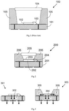
Vertical cavity surface emitting laser
PatentInactiveUS7110428B2
Innovation
- A VCSEL design featuring an active region, an electrical contact for injecting current, and an insulating region with an aperture between the active region and the contact, where the contact opening is larger than the aperture, allowing the direction of photon emission to be selectively determined by the injection current, enabling improved steering capabilities.
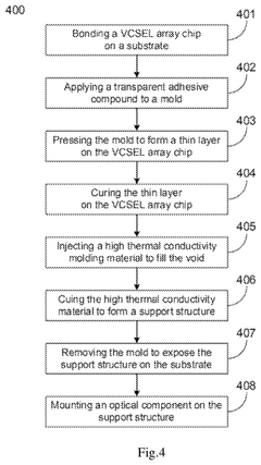
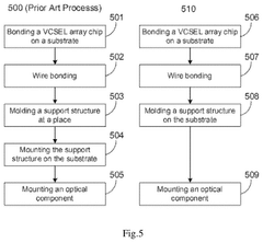
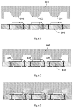
Vertical cavity surface emitting laser (VCSEL) array package and manufacturing method
PatentActiveUS12107387B2
Innovation
- A VCSEL array package design that includes a VCSEL array chip bonded on a substrate with a support structure molded from high thermal conductivity material, covering the side surfaces of the chip to create additional thermal paths and eliminate gaps, and a transparent thin layer to prevent beam obstruction and reflection.
Thermal Management Strategies for High-Performance VCSELs
Thermal management represents a critical challenge in VCSEL packaging for free-space optical interconnects, particularly as power densities continue to increase with advancing performance requirements. The thermal characteristics of VCSELs directly impact their reliability, wavelength stability, and overall performance metrics. Current high-performance VCSELs can generate significant heat during operation, with thermal densities exceeding 1 kW/cm² in advanced applications, necessitating sophisticated thermal management approaches.
Conventional thermal management strategies include the integration of heat sinks with optimized geometries to maximize surface area while maintaining compact form factors. These designs typically employ materials with high thermal conductivity such as copper (398 W/m·K) or aluminum (237 W/m·K), though advanced packaging increasingly utilizes diamond-based composites offering superior thermal conductivity (>1500 W/m·K) despite higher manufacturing costs.
Active cooling technologies have emerged as essential components for high-power VCSEL arrays. Thermoelectric coolers (TECs) provide precise temperature control through the Peltier effect, maintaining optimal operating temperatures within ±0.1°C. Micro-channel liquid cooling systems represent another advanced approach, offering heat flux dissipation capabilities exceeding 500 W/cm² by circulating coolants through miniaturized channels directly beneath the VCSEL array.
Thermal interface materials (TIMs) play a crucial role in minimizing thermal resistance between the VCSEL and heat dissipation structures. Recent developments include metal-based TIMs with embedded nanoparticles achieving thermal conductivities of 20-50 W/m·K, significantly outperforming traditional polymer-based compounds (3-5 W/m·K).
Thermal simulation and modeling have become indispensable tools in VCSEL package design. Computational fluid dynamics (CFD) and finite element analysis (FEA) enable accurate prediction of thermal profiles and identification of potential hotspots before physical prototyping. These simulation approaches have demonstrated correlation with experimental measurements within 5-10% accuracy when properly calibrated.
Emerging thermal management innovations include phase-change materials that absorb heat during state transitions, providing thermal buffering during peak operation periods. Additionally, graphene-based thermal spreaders with in-plane thermal conductivity exceeding 3000 W/m·K are showing promise in laboratory settings, though manufacturing challenges currently limit commercial deployment.
The selection of appropriate thermal management strategies must balance performance requirements against size, weight, power consumption, and cost constraints specific to the intended free-space optical interconnect application.
Integration Standards and Interoperability Considerations
The integration of VCSEL-based free-space optical interconnects into existing systems requires adherence to established standards and careful consideration of interoperability factors. Currently, several industry consortia are working to develop standardized approaches for optical interconnect integration, including the Consortium for On-Board Optics (COBO) and the Optical Internetworking Forum (OIF). These organizations are establishing specifications for form factors, optical interfaces, and electrical signaling that enable seamless integration of VCSEL-based interconnects with existing electronic systems.
A critical aspect of integration standards involves the mechanical specifications for VCSEL packages. The industry is converging toward standardized dimensions and mounting configurations that facilitate automated assembly processes. For instance, the Common Management Interface Specification (CMIS) provides a framework for managing optical modules, including those based on VCSEL technology, ensuring consistent control interfaces across different vendors' implementations.
Interoperability between VCSEL-based interconnects and traditional copper or fiber-based systems presents significant challenges. Protocol translation layers are often required to ensure seamless data transfer between different interconnect technologies. The IEEE 802.3 working groups have developed standards that address these translation requirements, particularly for data center applications where hybrid interconnect solutions are increasingly common.
Thermal management considerations also factor into integration standards, with specifications defining acceptable operating temperature ranges and heat dissipation requirements. The JEDEC JC-15 committee has established thermal testing methodologies specifically applicable to optoelectronic packages, providing a standardized approach for evaluating VCSEL package thermal performance across different manufacturers.
Signal integrity standards are equally important, with specifications defining acceptable levels of jitter, crosstalk, and signal degradation. The OIF-CEI (Common Electrical I/O) specifications provide guidelines for electrical interfaces that connect to optical modules, ensuring consistent performance across different implementation scenarios. These standards are particularly relevant for high-speed applications where signal integrity directly impacts system performance.
Looking forward, emerging standards are beginning to address wavelength division multiplexing (WDM) capabilities in VCSEL-based interconnects, defining channel spacing and wavelength allocation schemes that maximize bandwidth while ensuring interoperability. The development of multi-vendor interoperability test procedures represents another important trend, with organizations like the University of New Hampshire InterOperability Laboratory (UNH-IOL) establishing certification programs specifically for free-space optical interconnect technologies.
Unlock deeper insights with Patsnap Eureka Quick Research — get a full tech report to explore trends and direct your research. Try now!
Generate Your Research Report Instantly with AI Agent
Supercharge your innovation with Patsnap Eureka AI Agent Platform!