What Challenges Exist in Silicon Micropillar Fabrication?
JUL 9, 20259 MIN READ
Generate Your Research Report Instantly with AI Agent
Patsnap Eureka helps you evaluate technical feasibility & market potential.
Silicon Micropillar Background and Objectives
Silicon micropillars have emerged as a crucial technology in various fields, including photonics, electronics, and energy harvesting. The development of these structures dates back to the early 2000s when researchers began exploring ways to enhance the performance of silicon-based devices through nanoscale engineering. As the semiconductor industry continues to push the boundaries of miniaturization, silicon micropillars have gained significant attention due to their unique properties and potential applications.
The evolution of silicon micropillar technology has been driven by the need for improved light absorption, enhanced electron mobility, and increased surface area in silicon-based devices. Initially, the focus was on creating simple pillar structures through etching techniques. However, as the field progressed, more sophisticated fabrication methods were developed, allowing for precise control over pillar dimensions, spacing, and surface characteristics.
One of the primary objectives in silicon micropillar research is to overcome the limitations of traditional planar silicon structures. By creating three-dimensional architectures, researchers aim to enhance light trapping and carrier collection in photovoltaic cells, improve heat dissipation in electronic devices, and increase the sensitivity of sensors. Additionally, silicon micropillars offer the potential for integrating multiple functionalities within a single device, paving the way for more compact and efficient systems.
The current technological landscape surrounding silicon micropillars is characterized by a diverse range of fabrication techniques, including top-down approaches like reactive ion etching and bottom-up methods such as vapor-liquid-solid growth. Each approach presents its own set of challenges and opportunities, driving ongoing research to optimize fabrication processes and expand the range of achievable structures.
As the field continues to advance, several key objectives have emerged. These include developing scalable and cost-effective fabrication methods suitable for large-area production, improving the uniformity and reproducibility of micropillar arrays, and exploring novel surface treatments to enhance functionality. Furthermore, researchers are investigating ways to integrate silicon micropillars with other materials and technologies to create hybrid systems with enhanced performance characteristics.
The potential applications of silicon micropillars span a wide range of industries. In the solar energy sector, they offer the promise of higher efficiency photovoltaic cells. In electronics, they could enable the development of more powerful and energy-efficient devices. In the field of sensing and biomedical applications, silicon micropillars may lead to more sensitive and selective detection platforms.
Looking ahead, the trajectory of silicon micropillar technology is expected to intersect with other emerging fields, such as quantum computing and neuromorphic engineering. This convergence may open up new avenues for innovation and drive the development of next-generation devices and systems based on advanced silicon architectures.
Market Demand Analysis for Silicon Micropillars
The market demand for silicon micropillars has been steadily growing across various industries, driven by their unique properties and potential applications. In the semiconductor industry, silicon micropillars are gaining traction as a promising solution for next-generation electronic devices. These structures offer enhanced performance in areas such as heat dissipation, electrical conductivity, and mechanical strength, making them attractive for advanced chip designs and 3D integrated circuits.
The photovoltaic sector represents another significant market for silicon micropillars. As the global push for renewable energy intensifies, solar cell manufacturers are exploring ways to improve efficiency and reduce costs. Silicon micropillars have shown potential in enhancing light absorption and charge collection in solar cells, potentially leading to higher conversion efficiencies and lower production costs.
In the field of biomedical devices, silicon micropillars are finding applications in biosensors, drug delivery systems, and tissue engineering. Their high surface-to-volume ratio and biocompatibility make them ideal for developing sensitive and selective biosensors for disease detection and monitoring. The pharmaceutical industry is also exploring the use of silicon micropillars for controlled drug release and targeted delivery systems.
The emerging market of wearable technology and flexible electronics presents another avenue for silicon micropillar applications. These structures can be integrated into flexible substrates, enabling the development of bendable and stretchable electronic devices with improved durability and performance.
Market analysts project substantial growth in the silicon micropillar market over the next decade. The increasing demand for miniaturization in electronics, coupled with the need for more efficient energy harvesting and storage solutions, is expected to drive this growth. However, the market faces challenges in scaling up production and reducing manufacturing costs to meet mass-market demands.
The automotive industry is also showing interest in silicon micropillars for applications in sensors, battery technology, and lightweight structural components. As vehicles become more electrified and autonomous, the demand for advanced materials and sensors is expected to rise, potentially creating new opportunities for silicon micropillar technologies.
While the market potential is significant, widespread adoption of silicon micropillars will depend on overcoming current fabrication challenges and demonstrating clear advantages over existing technologies in terms of performance and cost-effectiveness. As research and development efforts continue to address these issues, the market for silicon micropillars is poised for expansion across multiple sectors.
Current Challenges in Micropillar Fabrication
Silicon micropillar fabrication faces several significant challenges that hinder its widespread adoption and optimization. One of the primary obstacles is achieving precise control over the micropillar dimensions and uniformity across large areas. The fabrication process requires nanometer-scale precision, which is difficult to maintain consistently over wafer-scale production.
Another major challenge lies in the etching process used to create the micropillars. Achieving high aspect ratios while maintaining vertical sidewalls is particularly demanding. Deep reactive ion etching (DRIE), a common technique used in micropillar fabrication, can lead to scalloping effects on the sidewalls, compromising the structural integrity and performance of the micropillars.
The choice of masking material and its patterning also present significant hurdles. The mask must withstand the aggressive etching processes while maintaining its integrity and dimensional stability. Conventional photoresists often struggle to meet these requirements, necessitating the exploration of alternative masking materials such as metal hard masks or advanced resist formulations.
Surface contamination and defects pose another set of challenges in micropillar fabrication. Even minor impurities or particulates can lead to significant defects in the final structure, affecting both the yield and performance of the devices. Maintaining ultra-clean environments and developing robust cleaning protocols are crucial but technically demanding aspects of the fabrication process.
The high aspect ratio of micropillars also introduces challenges in subsequent processing steps, such as conformal coating or filling of the structures. Ensuring uniform deposition or complete filling of high aspect ratio features without voids or defects requires careful optimization of deposition parameters and often necessitates the development of specialized techniques.
Stress management is another critical challenge in micropillar fabrication. The high surface-to-volume ratio of these structures makes them particularly susceptible to stress-induced deformation or collapse. Balancing the mechanical stability of the micropillars with their desired functional properties requires careful material selection and process optimization.
Finally, the scalability of micropillar fabrication processes for high-volume production remains a significant challenge. Many of the current fabrication techniques are time-consuming and not easily adaptable to large-scale manufacturing. Developing processes that can maintain the required precision and quality while increasing throughput is crucial for the commercial viability of micropillar-based technologies.
Existing Fabrication Methods and Limitations
01 Fabrication methods for silicon micropillars
Various techniques are employed to create silicon micropillars, including etching processes, lithography, and deposition methods. These fabrication methods allow for precise control over the size, shape, and arrangement of the micropillars, which is crucial for their performance in different applications.- Fabrication methods for silicon micropillars: Various techniques are employed to create silicon micropillars, including etching processes, lithography, and deposition methods. These fabrication methods allow for precise control over the size, shape, and arrangement of the micropillars, which is crucial for their performance in different applications.
- Applications in solar cells and photovoltaics: Silicon micropillars are utilized in solar cell and photovoltaic technologies to enhance light absorption and improve overall efficiency. The unique structure of micropillars allows for better light trapping and increased surface area, leading to improved energy conversion rates.
- Use in microfluidic devices and lab-on-a-chip systems: Silicon micropillars play a significant role in microfluidic devices and lab-on-a-chip systems. They can be used for fluid manipulation, particle separation, and as support structures for various biochemical processes, enhancing the functionality and efficiency of these miniaturized systems.
- Integration with sensors and MEMS devices: Silicon micropillars are integrated into various sensors and MEMS (Micro-Electro-Mechanical Systems) devices. Their unique properties allow for enhanced sensitivity, improved signal-to-noise ratios, and increased surface area for sensing applications, making them valuable in fields such as environmental monitoring and biomedical sensing.
- Surface modification and functionalization: The surface of silicon micropillars can be modified and functionalized to tailor their properties for specific applications. This includes coating with various materials, chemical treatments, and the addition of functional groups to enhance their performance in areas such as catalysis, biosensing, and energy storage.
02 Applications in solar cells and photovoltaics
Silicon micropillars are utilized in solar cell and photovoltaic technologies to enhance light absorption and improve overall efficiency. The unique structure of micropillars allows for better light trapping and increased surface area, leading to improved energy conversion rates.Expand Specific Solutions03 Use in microfluidic and lab-on-a-chip devices
Silicon micropillars play a significant role in microfluidic systems and lab-on-a-chip devices. They can be used for fluid manipulation, particle separation, and as structural elements in miniaturized analytical systems, enabling more efficient and precise analysis in various fields.Expand Specific Solutions04 Integration with sensors and MEMS devices
Silicon micropillars are integrated into various sensors and MEMS (Micro-Electro-Mechanical Systems) devices. Their unique properties allow for enhanced sensitivity in chemical and biological sensors, as well as improved performance in mechanical sensing applications.Expand Specific Solutions05 Surface modification and functionalization
The surface of silicon micropillars can be modified and functionalized to tailor their properties for specific applications. This includes coating with various materials, chemical treatments, and the addition of functional groups to enhance their performance in areas such as catalysis, sensing, and biomedical applications.Expand Specific Solutions
Key Players in Micropillar Manufacturing
The silicon micropillar fabrication industry is in a growth phase, with increasing demand driven by applications in semiconductor devices, energy storage, and advanced materials. The market size is expanding, fueled by the need for miniaturization and improved performance in various technologies. While the technology is maturing, challenges in precision manufacturing and scalability persist. Companies like Taiwan Semiconductor Manufacturing Co., Ltd. and Lam Research Corp. are at the forefront, leveraging their expertise in semiconductor fabrication. Emerging players such as Nanomakers SA and Microfabrica, Inc. are focusing on innovative approaches to overcome technical hurdles. Research institutions like Consiglio Nazionale delle Ricerche and Peking University are contributing to advancements in the field, pushing the boundaries of what's possible in silicon micropillar fabrication.
Wolfspeed, Inc.
Technical Solution: Wolfspeed specializes in silicon carbide (SiC) and gallium nitride (GaN) technologies, which involve challenges similar to silicon micropillar fabrication. For SiC devices, they've developed techniques to create high aspect ratio trenches and pillars in this harder material. Their process involves specialized plasma etching with high selectivity masks and tailored gas chemistries to achieve vertical sidewalls [10]. To address the challenge of high defect densities in SiC, Wolfspeed has implemented advanced epitaxial growth techniques and defect-reduction strategies. They've also developed unique doping methods for SiC pillars, including ion implantation and in-situ doping during growth. Wolfspeed's approach includes the use of high-temperature annealing processes to manage stress and improve electrical properties of the micropillar structures [11].
Strengths: Expertise in wide bandgap semiconductors, vertical integration from materials to devices. Weaknesses: Focused on specific materials (SiC, GaN) rather than traditional silicon.
Taiwan Semiconductor Manufacturing Co., Ltd.
Technical Solution: TSMC has developed advanced silicon micropillar fabrication techniques for 3D IC integration. They utilize Through-Silicon Vias (TSVs) to create high-density interconnects between stacked chips. Their process involves deep reactive ion etching (DRIE) to form high aspect ratio micropillars, followed by insulation and copper filling [1]. TSMC has achieved 7nm node TSV technology with diameters as small as 0.5μm and depths up to 100μm [2]. They've also implemented wafer thinning and temporary bonding techniques to handle ultra-thin wafers during processing. To address challenges like void formation and stress management, TSMC employs optimized deposition methods and annealing processes [3].
Strengths: Industry-leading process node, high-density integration capabilities. Weaknesses: High cost, complexity in managing thermal issues in 3D stacks.
Innovative Approaches in Micropillar Etching
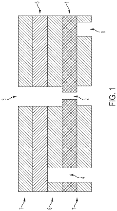
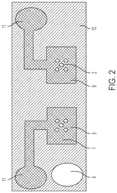
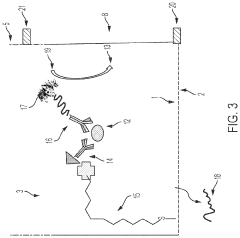
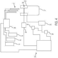
Microwell Microelectrode Filtration Sensor
PatentPendingUS20230408507A1
Innovation
- The development of analyte detection microwells with multiple layers, including a filtration membrane with pores as a reactive metal surface for the working electrode and non-reactive metal layers for counter and reference electrodes, allows for efficient biomolecule capture and detection under low hydrodynamic force, using inert materials like plastics or ceramics for the non-reactive layers and reactive metals like gold for the working electrode.
Method of forming a micromechanical structure
PatentInactiveUS20050057792A1
Innovation
- A hydrogen treatment is applied to the first sacrificial silicon layer to form an H-treated surface with Si—H bonds, which enhances the adhesion between the layers by replacing dangling bonds and improving impurity resistance, allowing for secure deposition of the second sacrificial silicon layer without peeling.
Material Science Advancements for Micropillars
Recent advancements in material science have significantly contributed to the development of silicon micropillars, addressing several key challenges in their fabrication process. One of the primary areas of focus has been improving the mechanical properties of silicon micropillars to enhance their durability and performance under various conditions.
Researchers have made substantial progress in developing novel silicon alloys and composites that exhibit superior strength and flexibility compared to pure silicon. These advanced materials allow for the creation of micropillars with improved structural integrity, reducing the risk of fracture during fabrication and subsequent use. Additionally, the incorporation of dopants and other elements into the silicon matrix has led to enhanced electrical and optical properties, expanding the potential applications of silicon micropillars in various fields.
Surface modification techniques have also seen significant advancements, enabling better control over the surface properties of silicon micropillars. Innovative coating methods, such as atomic layer deposition and plasma-enhanced chemical vapor deposition, have been developed to create ultra-thin, uniform layers on the micropillar surfaces. These coatings can impart specific functionalities, such as improved wettability, biocompatibility, or chemical resistance, tailoring the micropillars for specific applications.
Another area of progress has been in the development of hierarchical structures within silicon micropillars. By incorporating nanoscale features onto the micropillar surfaces, researchers have created multi-scale architectures that exhibit unique properties. These hierarchical structures can enhance surface area, improve light trapping in photovoltaic applications, and provide better control over cell adhesion in biomedical devices.
Material scientists have also made strides in understanding and mitigating the effects of stress and strain during the micropillar fabrication process. Advanced simulation techniques and in-situ characterization methods have provided valuable insights into the behavior of silicon at the microscale. This knowledge has led to the development of optimized fabrication protocols that minimize internal stresses and defects, resulting in more reliable and consistent micropillar structures.
Furthermore, the exploration of alternative silicon-based materials, such as silicon carbide and silicon nitride, has opened up new possibilities for micropillar fabrication. These materials offer enhanced thermal stability, chemical resistance, and mechanical strength compared to pure silicon, making them suitable for applications in harsh environments or high-temperature conditions.
In conclusion, material science advancements have played a crucial role in addressing the challenges associated with silicon micropillar fabrication. Through the development of novel materials, surface modification techniques, and improved understanding of material behavior at the microscale, researchers have significantly enhanced the performance and versatility of silicon micropillars. These advancements continue to drive innovation in various fields, including microelectronics, energy harvesting, and biomedical engineering.
Environmental Impact of Micropillar Production
The production of silicon micropillars, while offering significant technological advancements, raises important environmental concerns that must be addressed. The fabrication process involves several stages that can potentially impact the environment, including material extraction, energy consumption, and waste generation.
The primary environmental challenge in micropillar production is the intensive use of energy. The fabrication process requires high-temperature operations and precise control of environmental conditions, leading to substantial energy consumption. This energy demand often relies on fossil fuel-based power sources, contributing to greenhouse gas emissions and climate change. Efforts to transition to renewable energy sources for manufacturing facilities could significantly reduce this environmental footprint.
Another critical environmental issue is the use of hazardous chemicals in the fabrication process. Etching and cleaning steps often involve chemicals such as hydrofluoric acid, which can pose serious risks to both human health and the environment if not properly managed. Proper handling, storage, and disposal of these chemicals are essential to prevent soil and water contamination. Additionally, the production of silicon wafers, the base material for micropillars, involves water-intensive processes that can strain local water resources, particularly in water-scarce regions.
The generation of electronic waste (e-waste) is a growing concern as devices incorporating micropillars reach end-of-life. Improper disposal of these components can lead to the release of toxic materials into the environment. Developing effective recycling and recovery methods for micropillar-containing devices is crucial to mitigate this impact and promote a circular economy approach in the electronics industry.
Furthermore, the extraction of raw materials required for micropillar production, such as high-purity silicon, can have significant environmental impacts. Mining operations can lead to habitat destruction, soil erosion, and water pollution. Sustainable sourcing practices and the development of alternative materials could help address these upstream environmental challenges.
To mitigate these environmental impacts, the industry is exploring various strategies. These include implementing more energy-efficient manufacturing processes, developing green chemistry alternatives for hazardous chemicals, improving water recycling systems in production facilities, and designing products for easier disassembly and recycling. Additionally, life cycle assessments are being conducted to identify hotspots in the environmental impact of micropillar production, guiding targeted improvements throughout the supply chain.
As the demand for silicon micropillars continues to grow, addressing these environmental challenges becomes increasingly important. Balancing technological advancement with environmental stewardship will be crucial for the sustainable development of this promising technology.
Unlock deeper insights with Patsnap Eureka Quick Research — get a full tech report to explore trends and direct your research. Try now!
Generate Your Research Report Instantly with AI Agent
Supercharge your innovation with Patsnap Eureka AI Agent Platform!