LED package with a rounded square lens

A LED device and lens technology, applied in the field of light-emitting diode (LED) packaging, can solve the problems of not being able to increase the diameter of the hemispherical lens, increase the width of the package 10, etc.

Active Publication Date: 2013-01-09
LUMILEDS HLDG BV
View PDF7 Cites 1 Cited by
  • Summary
  • Abstract
  • Description
  • Claims
  • Application Information

AI Technical Summary

Problems solved by technology

It is not possible to increase the diameter of the hemisphe

Method used


Image

  • LED package with a rounded square lens
  • LED package with a rounded square lens
  • LED package with a rounded square lens

Examples


Embodiment Construction

[0026] Figure 5-8 The invention is shown.

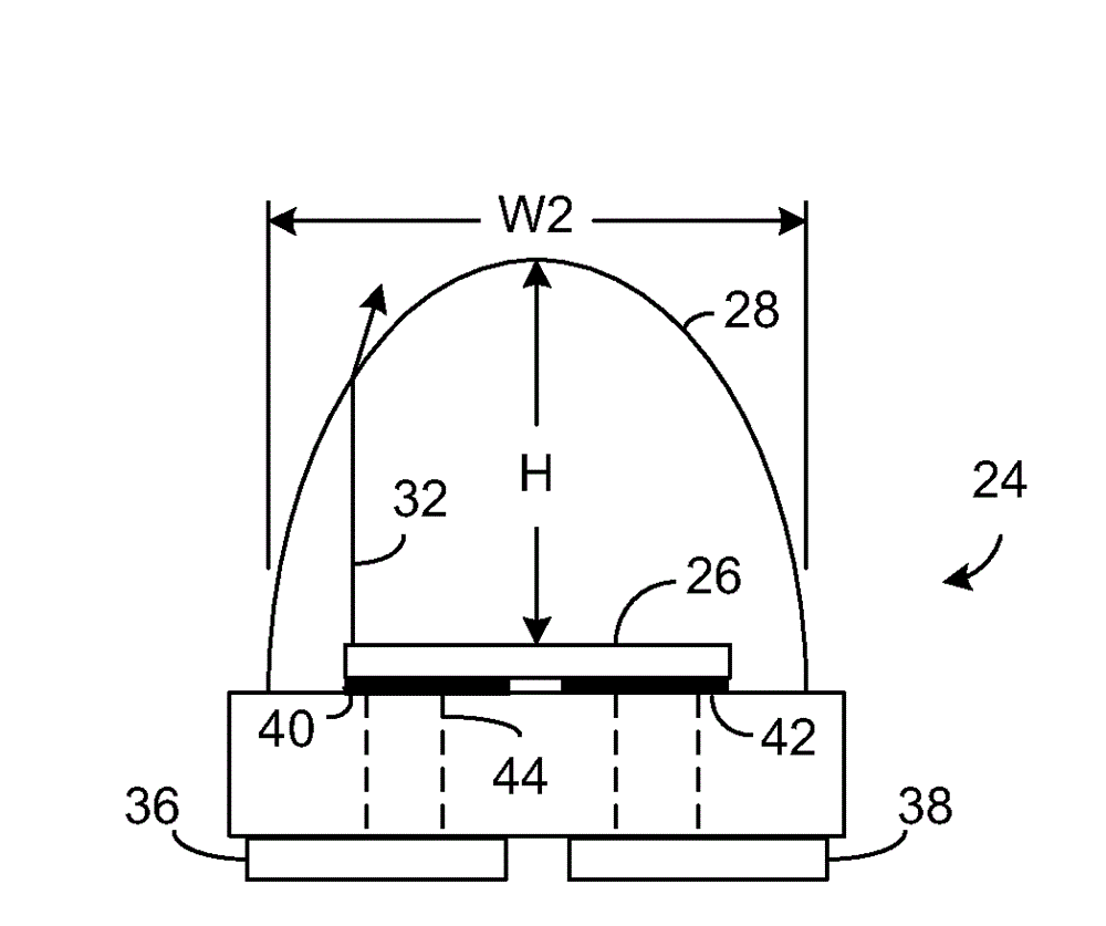
[0027] exist Figure 5-7 In this case, the body 22 of the package 24 may be ceramic, plastic, silicone or other material. The outer dimensions of the body 22 can be exactly the same as those of the prior art package 10 or 20, and the electrode structure can be exactly the same, so that the package 24 can be used instead of the package 10 or 20 in any application. The only difference is the size of the LED die 26 and lens 28 . In one example, LED die 26 includes an LED semiconductor layer mounted on a ceramic submount with a metal pattern, and electrodes on the submount are connected to package electrodes, as discussed with reference to FIG. 1 . In another embodiment, LED die 26 does not include a submount.

[0028] In a practical example, the diameter of the prior art hemispherical lens 12 in FIGS. 1 and 4 is about 2.55mm, Figure 5 The width of the rounded square lens 28 is the same size so that it can be used in a package of t...


PUM

PropertyMeasurementUnit
Widthaaaaaaaaaa

Abstract

A rounded square lens is used instead of a hemispherical lens in an LED package to produce a substantially Lambertian light emission pattern. A cross-sectional view of the rounded square lens cut along its diagonal forms a semicircular surface so as to emulate a hemispherical lens in areas close to the diagonal. A cross-sectional view of the lens cut along its width bisecting the lens forms a bullet shaped surface narrower than the semicircular surface but having the same height as the semicircular surface. The four corners of the lens are rounded. The surface of the lens smoothly transitions between the two surface shapes. Since the rounded square lens has a diagonal dimension larger than a maximum allowable diameter of a hemispherical lens in the same package body, a larger LED die may be used with the rounded square lens to output more light without increasing the size of the package while maintaining a Lambertian emission.

Description

technical field [0001] The present invention relates to light emitting diode (LED) packages, and more particularly, to LED packages with rounded square lenses emitting a substantially Lambertian emission pattern. Background technique [0002] Prior Art Figure 1 is a top perspective view of an LED package 10 copied from the present assignee's US Design Patent No. D 598871, which is incorporated herein by reference. The trade name for this package is Rebel TM . Package 10 is approximately 3mm on each side. Package 10 contains a square LED die whose sides are aligned with the sides of package 10 . The central axis of the LED die is along the central axis of the hemispherical lens 12 . Anode and cathode electrodes are on the bottom surface of the package 10 for soldering to metal pads on the printed circuit board. The anode and cathode electrodes formed on the semiconductor layer of the LED are electrically connected to the anode and cathode electrodes on the bottom of the ...

Claims


Application Information

Patent Timeline
IPC IPC(8): H01L33/58H01L33/54G02B27/09H01L33/48
CPCH01L33/58G02B19/0061H01L2924/0002H01L33/486G02B27/0916G02B19/0014H01L33/54H01L2924/00H01L33/48
Inventor M.布特沃思
Owner LUMILEDS HLDG BV
Why Eureka
Try Eureka