Semiconductor structure, manufacturing method for semiconductor structure and operating method for semiconductor structure

A technology of manufacturing method and operation method, applied in semiconductor/solid-state device manufacturing, semiconductor device, electric solid-state device, etc., can solve problems such as reduction of electronic storage space and reduction of reliability of storage unit.

Active Publication Date: 2014-02-12
MACRONIX INT CO LTD
View PDF6 Cites 0 Cited by
  • Summary
  • Abstract
  • Description
  • Claims
  • Application Information

AI Technical Summary

Problems solved by technology

However, as the size of the storage device decreases, it is easy to cause the electronic storage space to decrease, and the reliability of the storage unit to decrease

Method used


Image

  • Semiconductor structure, manufacturing method for semiconductor structure and operating method for semiconductor structure
  • Semiconductor structure, manufacturing method for semiconductor structure and operating method for semiconductor structure
  • Semiconductor structure, manufacturing method for semiconductor structure and operating method for semiconductor structure

Examples


Embodiment Construction

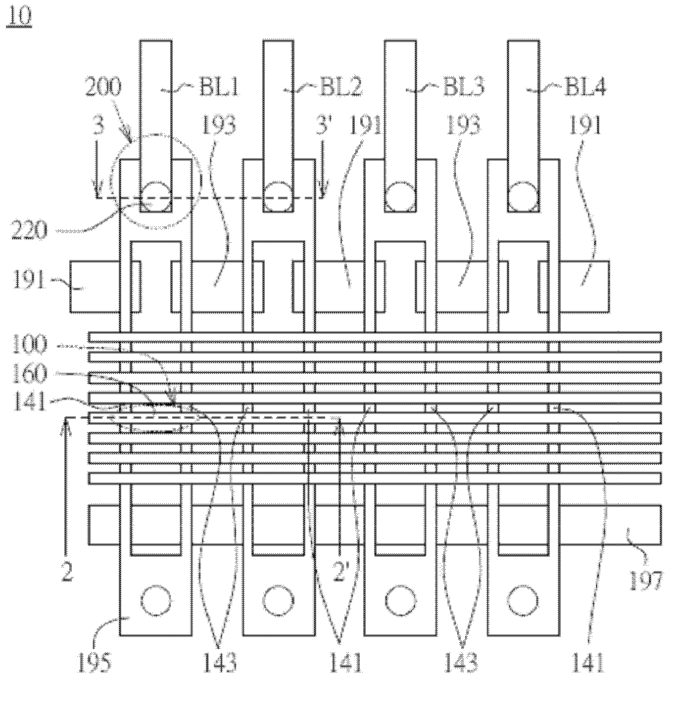
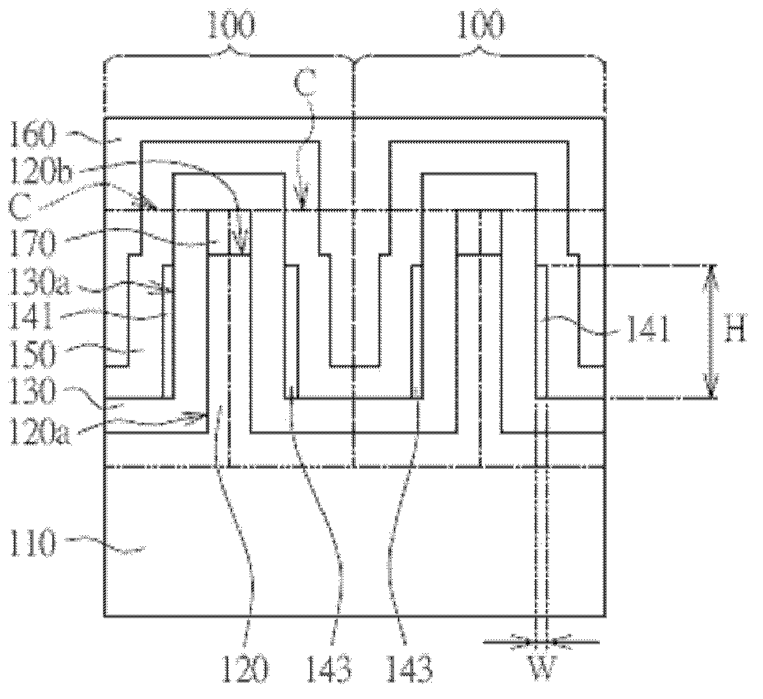
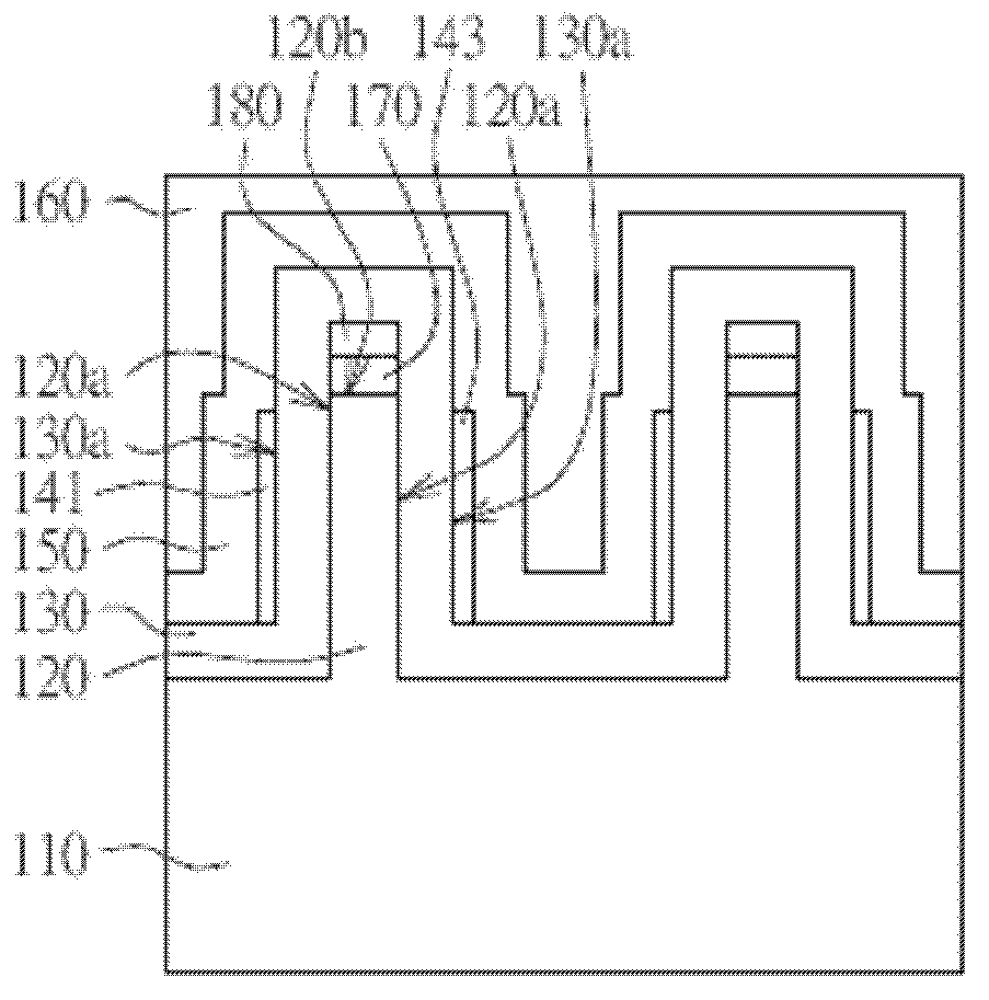
[0052] In the embodiments of the present invention, a semiconductor structure and its manufacturing method and operation method are provided. The first strip-shaped conductive block and the second strip-shaped conductive block of the semiconductor structure are respectively formed on the two side walls of a main structure, which can effectively increase the memory storage capacity per unit area in the horizontal direction, and maintain sufficient memory storage capacity to be effective The size miniaturization of the storage device is achieved, and the operation control and operation reliability of the storage device are improved. However, the detailed structures, process steps and operation steps proposed in the embodiments are for illustration purposes only, and are not intended to limit the protection scope of the present invention. The various steps are for illustration only, and are not intended to limit the present invention. Those with ordinary knowledge can modify or ...


PUM


Abstract

The invention discloses a semiconductor structure, a manufacturing method for the semiconductor and an operating method for the semiconductor structure. The semiconductor structure comprises a substrate, a main body structure, a main body structure, a first dielectric layer, a first strip-shaped conductive block, a second strip-shaped conductive block, a second dielectric layer and a conductive structure. The main body structure is formed on the substrate, the first dielectric layer is formed on the substrate and surrounds the two lateral walls and the top of the main body structure, the first strip-shaped conductive block and the second strip-shaped conductive block are respectively formed on the two lateral walls of the first dielectric layer, the second dielectric layer is formed on the first dielectric layer, the first strip-shaped conductive block and the second strip-shaped conductive block, and the conductive structure is formed on the second dielectric layer.

Description

technical field [0001] The present invention relates to a semiconductor structure and its manufacturing method and operating method, and in particular to a semiconductor structure for a memory device and its manufacturing method and operating method. Background technique [0002] In recent years, the structure of semiconductor devices has been constantly changing, and the memory storage capacity of the devices has also been increasing. Storage devices are used in many products, such as storage elements in MP3 players, digital cameras, computer files, and so on. With the increase of applications, the demand for storage devices also tends to be smaller in size and larger in storage capacity. However, as the size of the storage device decreases, the electronic storage space tends to decrease, and the reliability of the storage unit decreases. [0003] Therefore, designers are devoting themselves to developing and researching storage devices with reduced size, and improving th...

Claims


Application Information

Patent Timeline
Patent Type & Authority Applications(China)
IPC IPC(8): H01L27/115H01L21/8247
Inventor 陈士弘吕函庭
Owner MACRONIX INT CO LTD
Why Eureka
Try Eureka