
Volatile memory and fabricating method thereof
A non-volatile, manufacturing method technology, applied in semiconductor/solid-state device manufacturing, electrical solid-state devices, semiconductor devices, etc., can solve problems such as inconvenience, impact on memory operation margin, component performance, impact, etc.
- Summary
- Abstract
- Description
- Claims
- Application Information
AI Technical Summary
Problems solved by technology
Method used
Image

Examples
Embodiment Construction
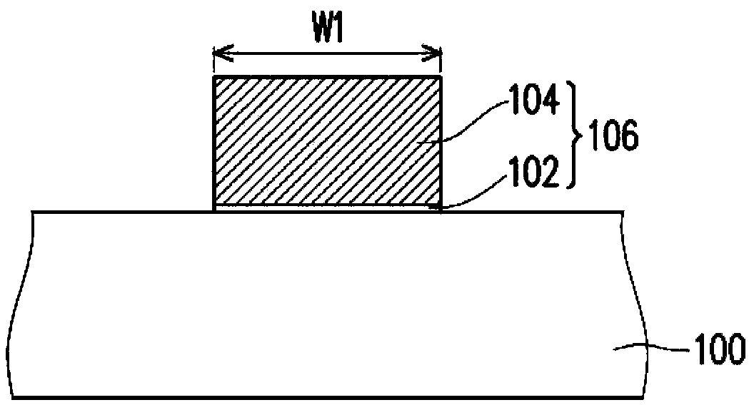
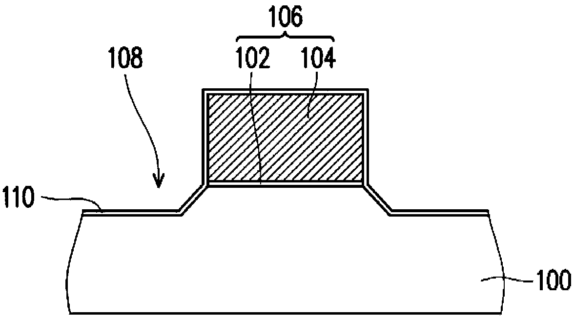
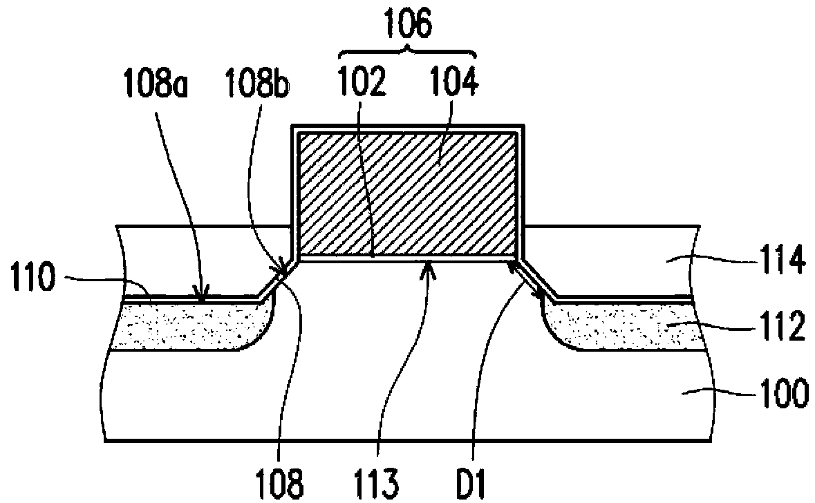
[0037] In order to further explain the technical means and effects of the present invention to achieve the intended purpose of the invention, the specific implementation and structure of the non-volatile memory and its manufacturing method according to the present invention will be described below in conjunction with the accompanying drawings and preferred embodiments. , method, step, feature and effect thereof, detailed description is as follows.
[0038] The aforementioned and other technical contents, features and effects of the present invention will be clearly presented in the following detailed description of preferred embodiments with reference to the drawings. Through the description of specific embodiments, it should be possible to obtain a deeper and more specific understanding of the technical means and effects of the present invention to achieve the intended purpose, but the attached drawings are only for reference and description, and are not used to explain the pr...
PUM
 Abstract
Description
Claims
Application Information