
Nonvolatile memory devices and methods of fabricating the same
A non-volatile storage and charge storage layer technology, which is applied in semiconductor/solid-state device manufacturing, electrical components, electric solid-state devices, etc., can solve the problems of difficult control of MLC operation scheme and difficult control of charge amount
Patent Information
- Authority / Receiving Office
- CN · China
- Patent Type
- Applications(China)
- Current Assignee / Owner
- Publication Date
- 2008-08-20
- Estimated Expiration
- Not applicable · inactive patent
Smart Images
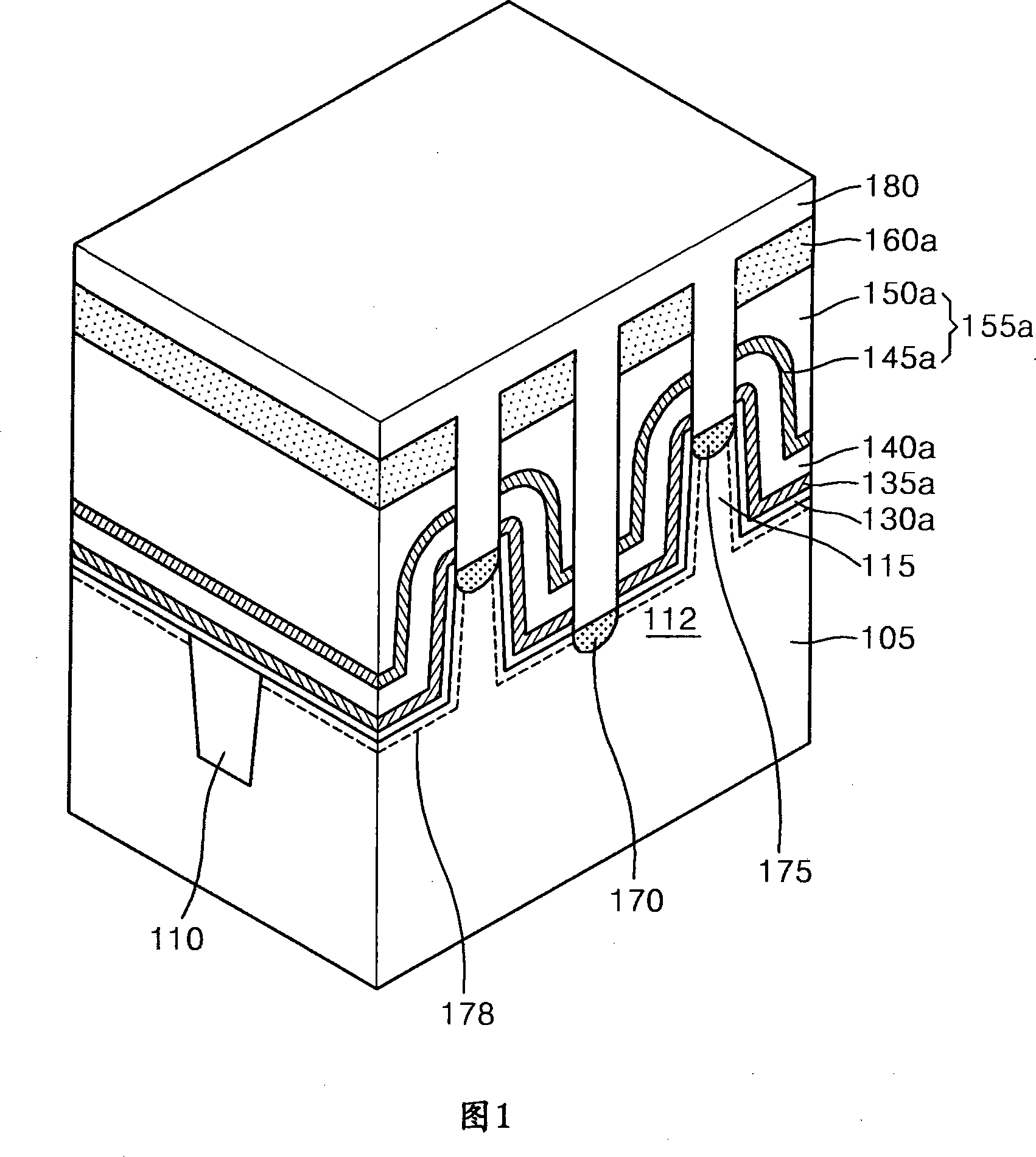
Figure 1 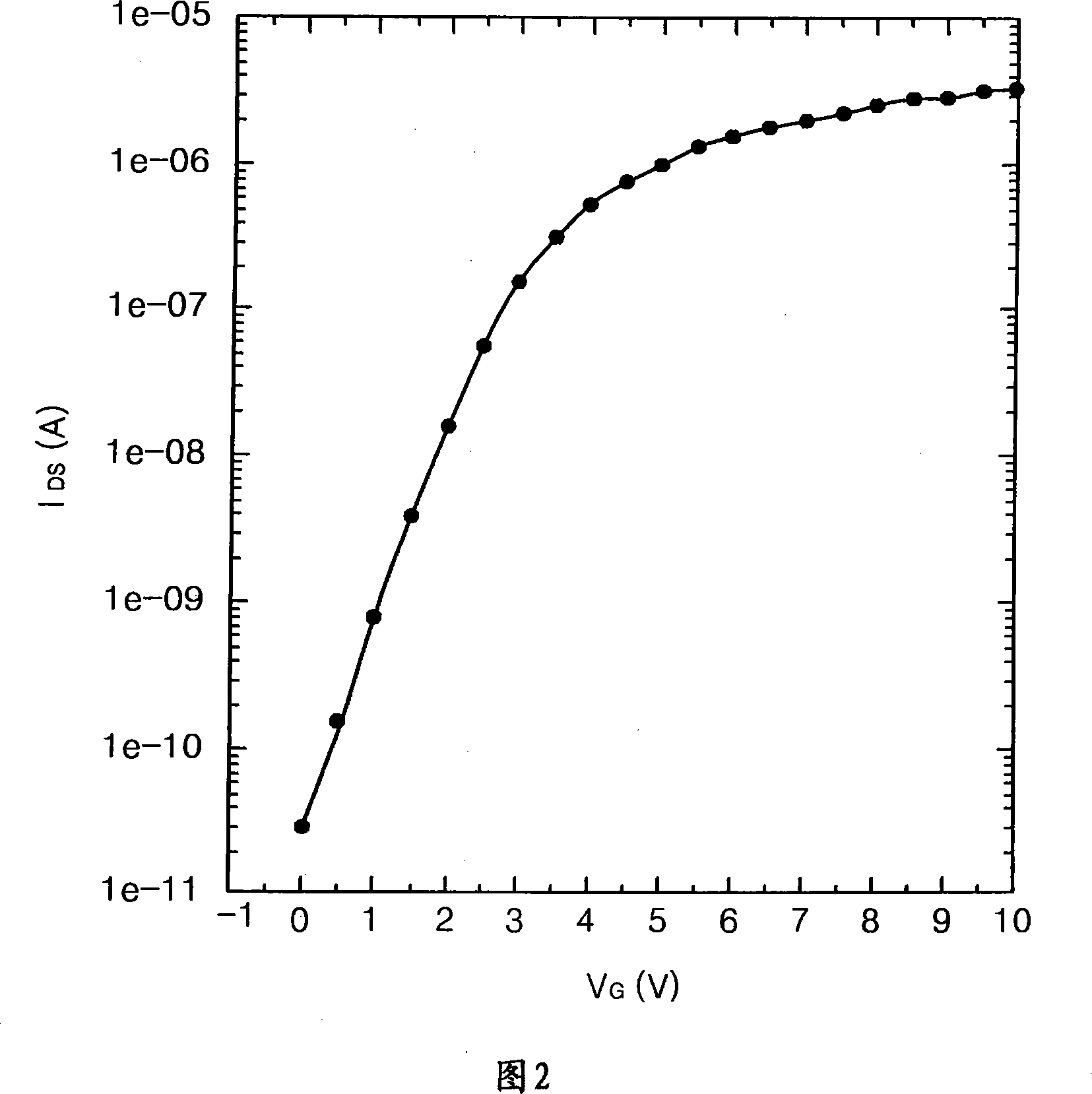
Figure 2 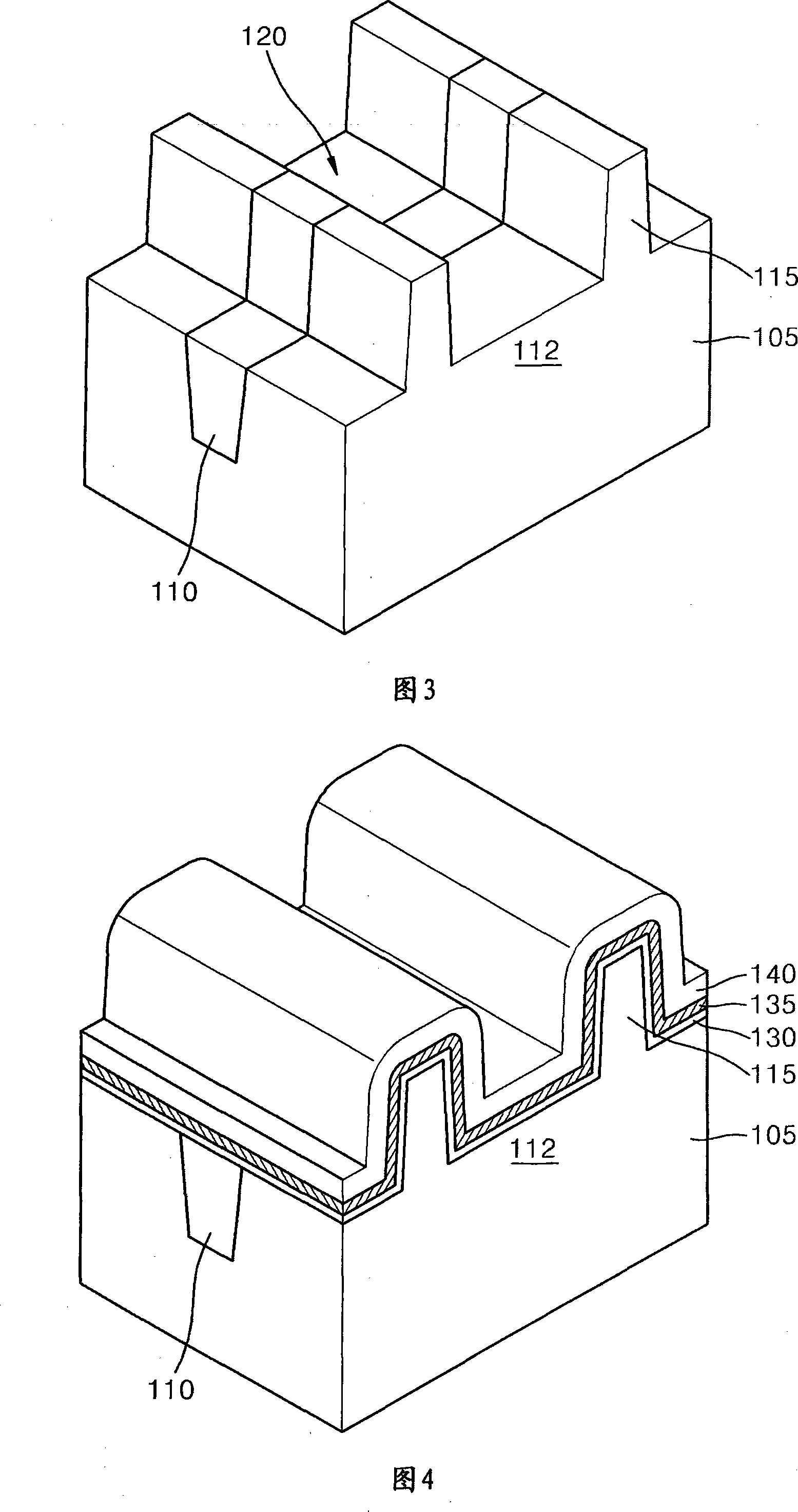
Figure 3
Abstract
Description
technical field
[0001] Example embodiments relate to a semiconductor device and a method of manufacturing the same. Other example embodiments relate to a nonvolatile memory device storing data using a charge storage layer and a method of manufacturing the same. Background technique
[0002] As the integration level of nonvolatile memory devices (eg, flash memory devices) increases, the channel length of the nonvolatile memory devices decreases, resulting in short channel effects. For example, the off-current of the flash memory device increases due to the punch-through effect, and the threshold voltage of the flash memory device decreases.
[0003] In order to suppress such a short channel effect, a method of increasing the impurity concentration in the body of the flash memory device may be used. However, such an increase in impurity concentration causes an increase in junction leakage current, which prevents or reduces channel voltage boosting. ...
Examples
Embodiment Construction
[0016] Example embodiments will now be described more fully hereinafter with reference to the accompanying drawings, in which example embodiments are shown. Example embodiments may, however, be embodied in many different forms and should not be construed as limited to the embodiments set forth herein. Rather, these embodiments are provided so that this disclosure will be thorough and complete, and will fully convey the scope of the example embodiments to those skilled in the art. In the drawings, the thicknesses of layers and regions are exaggerated for clarity. The same reference numerals denote the same elements.
[0017] It will be understood that when an element or layer is referred to as being on, connected to, or coupled to another element or layer, it can be directly on the other element or layer. , directly connected to or bonded to another element or layer, or intervening elements or layers may be present. In contrast, when an element is referred to as being direct...