Array substrate, display panel and display device

A technology for array substrates and display panels, applied in instruments, nonlinear optics, optics, etc., can solve problems that affect the performance of thin-film transistors, and achieve the effect of improving image display quality and performance

Inactive Publication Date: 2015-06-24
BOE TECH GRP CO LTD +1
View PDF6 Cites 7 Cited by
  • Summary
  • Abstract
  • Description
  • Claims
  • Application Information

AI Technical Summary

Problems solved by technology

[0004] The invention provides an array substrate, a display panel and a display device, which are used to solve the problem that the light reflected by the color filter substrate will affect the performance of the thin film transistor

Method used


Image

  • Array substrate, display panel and display device
  • Array substrate, display panel and display device
  • Array substrate, display panel and display device

Examples


Embodiment Construction

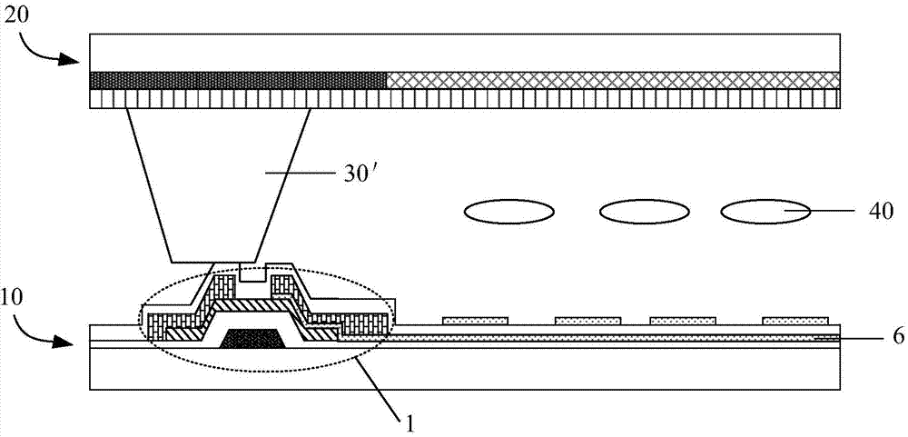
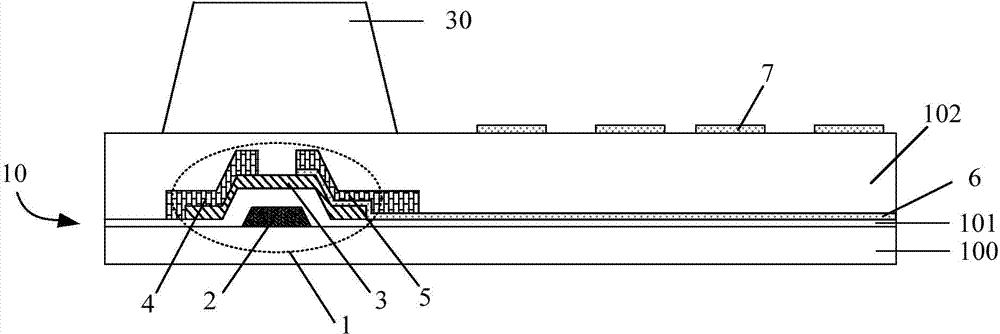
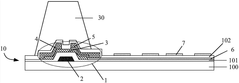
[0025] The present invention provides a liquid crystal panel. The liquid crystal panel includes a color filter substrate and an array substrate sealed to each other, and a spacer between the color filter substrate and the array substrate. The spacer is used to support the panel. The cell is thick, and the liquid crystal molecules fill the sealed space between the color filter substrate and the array substrate.

[0026] The array substrate includes a thin film transistor disposed on the base substrate, by setting the projection of the thin film transistor on the base substrate to completely fall into the projection of the spacer on the base substrate, so that the spacer The material can block the light reflected by the color filter substrate from irradiating the thin film transistor, thereby improving the performance of the thin film transistor and improving the picture display quality of the display device.

[0027] The spacer can be arranged on the color filter substrate or o...


PUM


Abstract

The invention relates to the technical field of display and discloses an array substrate, a display panel and a display device. A liquid crystal panel comprises an array substrate and a color-film substrate which are combined oppositely, and further comprises cushion arranged between the array substrate and the color-film substrate, and the array substrate comprises a thin-film transistor arranged on a substrate base plate. By setting projection of the thin-film transistor on the substrate base plate completely on the projection of the cushion on the substrate base plate, the cushion can protect the thin-film transistor from being irradiated by light rays reflected by the color-film substrate, performance of the thin-film transistor is improved and display quality of images of the display device is also improved.

Description

technical field [0001] The present invention relates to the field of display technology, in particular to an array substrate, a display panel and a display device. Background technique [0002] Thin Film Transistor-Liquid Crystal Display (TFT-LCD) has the characteristics of small size, low power consumption, and no radiation. It has developed rapidly in recent years and occupies a dominant position in the current flat panel display market. The main structure of the liquid crystal display is a liquid crystal panel, such as figure 1 As shown, the liquid crystal panel includes an array substrate 10 and a color filter substrate 20 arranged opposite to each other, and a liquid crystal layer 40 filled between the array substrate 10 and the color filter substrate 20 . The cell thickness of the liquid crystal panel is mainly controlled by a spacer (PS) 30 ′ formed between the array substrate 10 and the color filter substrate 20 . Wherein, a data line and a gate line (not shown in ...

Claims


Application Information

Patent Timeline
Patent Type & Authority Applications(China)
IPC IPC(8): G02F1/1339G02F1/1335G02F1/1333
CPCG02F1/133512G02F1/1339G02F1/13398
Inventor 朱亚文莫再隆樊浩原胡伟周全国
Owner BOE TECH GRP CO LTD
Why Eureka
Try Eureka