

Ultrathin wave-absorbing material anti-metal electronic label
A technology of wave absorbing material and electronic label, which is applied to record carriers, instruments, computer parts, etc. used in machines. It can solve the problems of decreasing reading and writing distance, inability to read, and weakening the electromagnetic field energy of the reader, so as to achieve a wide range of applications. , the effect of reducing loss and reducing probability
- Summary
- Abstract
- Description
- Claims
- Application Information
AI Technical Summary
Problems solved by technology
Method used
Image

Examples
Embodiment Construction
[0013] The present invention will be further described below in conjunction with the drawings and descriptions of the drawings.
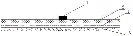
[0014] Such as figure 1 As shown, an ultra-thin wave-absorbing material anti-metal electronic tag is characterized in that it includes a chip 1, an aluminum-etched antenna 2, and a wave-absorbing material 3, the chip 1 is connected to the aluminum-etched antenna 2, the aluminum-etched antenna 2, and the wave-absorbing material 3 is bonded and connected through the adhesive layer 4; the frequency band of the chip 1 is 13.56MH or 860MHz-960MHz; the thickness of the wave-absorbing material 3 is 0.15-0.35mm. The overall thickness of the aluminum etched antenna 2 and the wave-absorbing material 3 is less than 0.7mm, and can be printed by a barcode printer.
PUM
| Property | Measurement | Unit |
|---|---|---|
| Thickness | aaaaa | aaaaa |
| Thickness | aaaaa | aaaaa |
Abstract
Description
Claims
Application Information