Array substrate and preparing method thereof, display panel and display device

A technology for array substrates and manufacturing methods, applied in the fields of array substrates and manufacturing methods thereof, display panels, and display devices, capable of solving the problems of high product cost and low degree of integrated control

Active Publication Date: 2017-10-20
BOE TECH GRP CO LTD +1
View PDF5 Cites 15 Cited by
  • Summary
  • Abstract
  • Description
  • Claims
  • Application Information

AI Technical Summary

Problems solved by technology

[0003] Taking the application of fingerprint recognition in the field of display devices, such as mobile phones or tablet computers, as an example, it can be used to authenticate and identify users; device, and then assembled with the display device, wherein the display device and the fingerprint identification device are controlled separately, resulting in higher product cost and lower degree of integrated control

Method used


Image

  • Array substrate and preparing method thereof, display panel and display device
  • Array substrate and preparing method thereof, display panel and display device
  • Array substrate and preparing method thereof, display panel and display device

Examples


Embodiment Construction

[0039] The following will clearly and completely describe the technical solutions in the embodiments of the present invention with reference to the accompanying drawings in the embodiments of the present invention. Obviously, the described embodiments are only some, not all, embodiments of the present invention. Based on the embodiments of the present invention, all other embodiments obtained by persons of ordinary skill in the art without making creative efforts belong to the protection scope of the present invention.

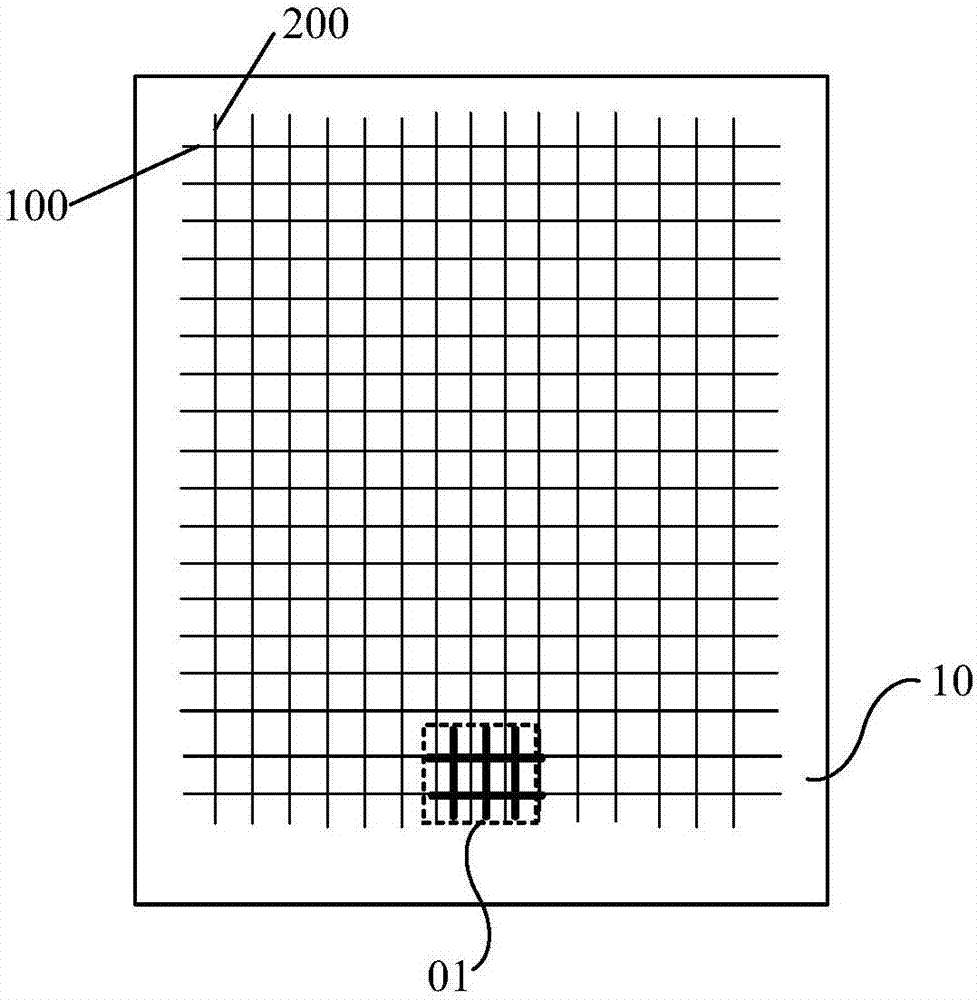
[0040] An embodiment of the present invention provides an array substrate, such as figure 1 As shown, it includes gate lines 100 and data lines 200 disposed on a base substrate 10 , and the array substrate has a fingerprint recognition area 01 .

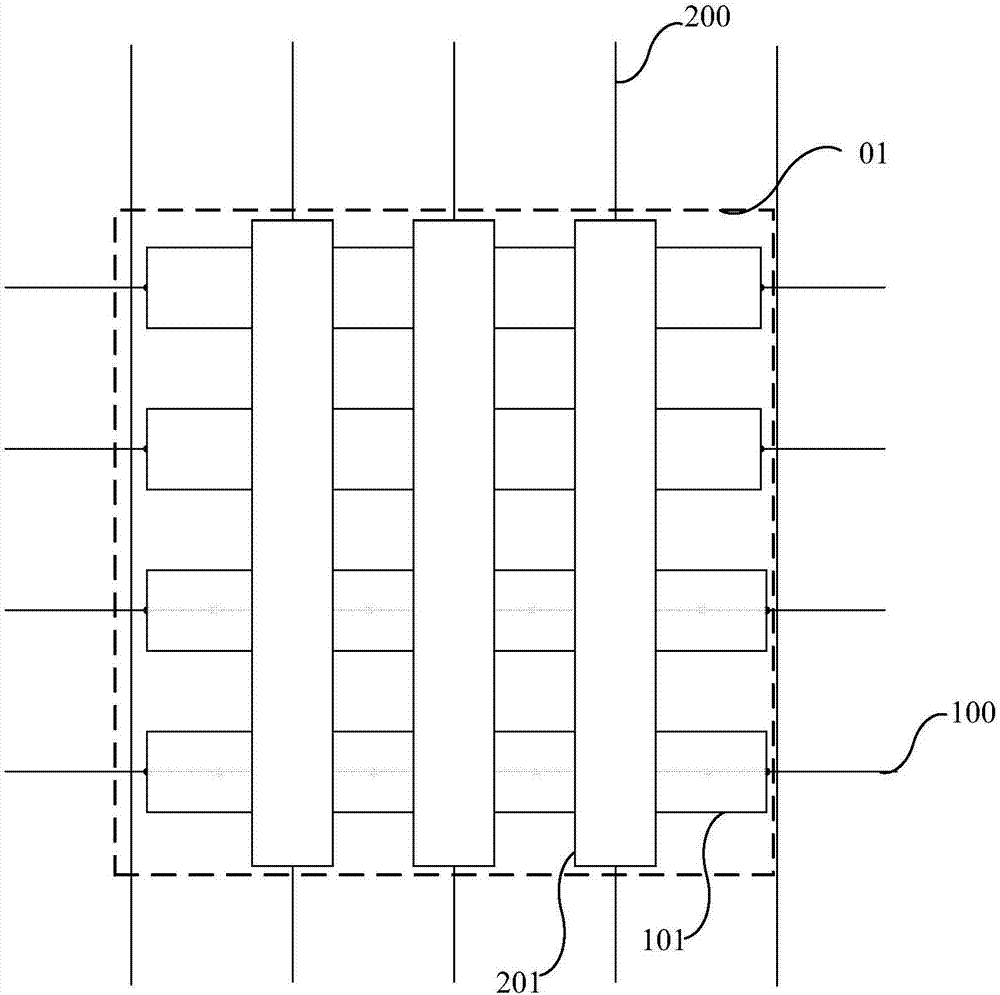
[0041] Specifically, such as figure 2 As shown, the array substrate includes in the fingerprint identification area 01: a plurality of emitting electrodes 101 and a plurality of sensing electrodes 201 intersecting ...


PUM


Abstract

The embodiment of the invention provides an array substrate and a preparing method thereof, a display panel and a display device, and relates to the technical field of fingerprint recognition. By integrating a fingerprint recognition device in the array substrate, the integrated control degree of the display device which comprises the fingerprint recognition device is increased. The array substrate comprises a data cable and a grid line which are arranged on a substrate, and is provided with a fingerprint recognition area; the fingerprint recognition area comprises multiple transmitting electrodes and sensing electrodes, wherein the transmitting electrodes and the sensing electrodes are arranged in a staggered mode, the sensing electrodes are located at the sides, deviating from the substrate, of the transmitting electrodes, and each transmitting electrode is electrically connected with the corresponding grid line.

Description

technical field [0001] The invention relates to the technical field of fingerprint identification, in particular to an array substrate and a manufacturing method thereof, a display panel, and a display device. Background technique [0002] Fingerprints are lines formed by raised (ridges) and sunken (valleys) skin on the pads of human fingers. It is naturally formed in the process of human evolution. Due to the lifelong invariance, uniqueness and convenience of fingerprints, etc. Therefore, it has become synonymous with biometric identification and is widely used in the fields of identity information authentication and identification such as security and attendance. [0003] Taking the application of fingerprint recognition in the field of display devices, such as mobile phones or tablet computers, as an example, it can be used to authenticate and identify users; The device is then assembled with the display device, wherein the display device and the fingerprint identificati...

Claims


Application Information

Patent Timeline
Patent Type & Authority Applications(China)
IPC IPC(8): G02F1/1333H01L27/32G06K9/00
CPCG02F1/1333G06V40/13H10K59/00G02F1/13338G06V40/1318H10K59/131G02F1/136286G02F1/136218G06V40/1306H10K59/40H10K59/126H10K59/1201
Inventor 孙世成王志强王培霍培荣胡双
Owner BOE TECH GRP CO LTD
Why Eureka
Try Eureka