OLED package substrate and manufacturing method thereof and OLED display panel

A technology for packaging substrates and manufacturing methods, which is applied to electrical components, electrical solid-state devices, circuits, etc., and can solve the problems of easy breakage of the contact electrode layer, disconnection of the auxiliary electrode pattern between the electrode layer and the auxiliary electrode layer, etc.

Active Publication Date: 2018-02-09
BOE TECH GRP CO LTD
View PDF5 Cites 9 Cited by
  • Summary
  • Abstract
  • Description
  • Claims
  • Application Information

AI Technical Summary

Problems solved by technology

[0004] Embodiments of the present invention provide an OLED encapsulation substrate and its manufacturing method, and an OLED display panel, which can solve the gap between the electrode layer and the auxiliary electrode pattern of the auxiliary electrode layer caused by the easy breakage of the contact electrode layer covered on the spacer in the prior art. intermittent road problem

Method used


Image

  • OLED package substrate and manufacturing method thereof and OLED display panel
  • OLED package substrate and manufacturing method thereof and OLED display panel
  • OLED package substrate and manufacturing method thereof and OLED display panel

Examples


Embodiment Construction

[0045] The following will clearly and completely describe the technical solutions in the embodiments of the present invention with reference to the accompanying drawings in the embodiments of the present invention. Obviously, the described embodiments are only some, not all, embodiments of the present invention. Based on the embodiments of the present invention, all other embodiments obtained by persons of ordinary skill in the art without making creative efforts belong to the protection scope of the present invention.

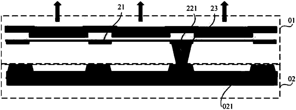
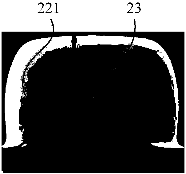
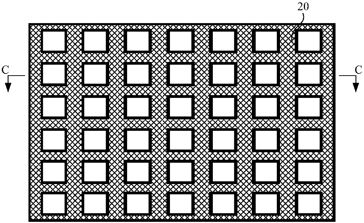
[0046] An embodiment of the present invention provides an OLED packaging substrate, such as Figure 4 As shown, a base substrate 10 is included, and the base substrate 10 includes a pixel-corresponding area A and a pixel-defining corresponding area B. A conductive structure 20 is arranged on the base substrate 10, and the projection of the conductive structure 20 on the base substrate 10 is located at the pixel-defining area. Corresponding to area B, such as ...


PUM


Abstract

The embodiment of the invention provides an OLED package substrate and a manufacturing method thereof and an OLED display panel, relates to the technical field of display and aims at solving the problem that a contact electrode layer covering a spacer is easy to break to cause disconnection of the electrode layer and an auxiliary electrode pattern of an auxiliary electrode layer in the prior art.The provided OLED package substrate comprises a substrate, wherein the substrate comprises a pixel corresponding region and a pixel definition corresponding region; the substrate is provided with conductive structures; projections of the conductive structures on the substrate are located in the pixel definition corresponding region; and a transparent insulating layer is arranged between the conductive structures.

Description

technical field [0001] The invention relates to the field of display technology, in particular to an OLED packaging substrate, a manufacturing method thereof, and an OLED display panel. Background technique [0002] With the development and progress of display technology, for existing display devices, organic light emitting diode (Organic Light Emitting Diode, OLED) is a current-mode light-emitting device, because of its self-luminescence, fast response , wide viewing angle and flexible display, etc., are increasingly being used in the field of high-performance display. [0003] For top-emitting organic light-emitting diode devices, such as figure 1 As shown, the light emitted by the organic light-emitting layer exits through one side of the OLED packaging substrate 01 (such as figure 1 The direction indicated by the middle arrow), in order to make the top-emission organic electroluminescent diode have better light transmittance, the thickness of the electrode layer 021 on...

Claims


Application Information

Patent Timeline
Patent Type & Authority Applications(China)
IPC IPC(8): H01L27/32
CPCH10K59/131H10K59/1201
Inventor 李伟张星
Owner BOE TECH GRP CO LTD
Why Eureka
Try Eureka