Electronic component grounding device and method

A technology of electronic components and grounding devices, applied in the direction of connecting parts protective grounding/shielding devices, electrical components, circuit/current collector components, etc., can solve problems such as short-circuit damage, poor grounding effect, poor grounding, etc., to avoid short-circuit Damage, ease of installation, reduced process effects

Active Publication Date: 2018-03-23
成都芯通软件有限公司
View PDF6 Cites 2 Cited by
  • Summary
  • Abstract
  • Description
  • Claims
  • Application Information

AI Technical Summary

Problems solved by technology

[0004] The purpose of the present invention is to provide a grounding device and a grounding method for electronic components, aiming at the problem that the grounding effect is poor and short-circuit damage is prone to occur due to poor contact between the two when the electronic components are installed on the circuit board. The grounding device has a notch on the PCB board, so that the electronic components are in close contact with the PCB board through the grounding reed, which solves the problem of poor grounding of the electronic components installed on the circuit board in the prior art, and makes the electronic components convenient. Installed on the PCB board to achieve a good grounding effect and ensure the operation and safety of electronic components

Method used


Image

  • Electronic component grounding device and method
  • Electronic component grounding device and method
  • Electronic component grounding device and method

Examples


Embodiment 1

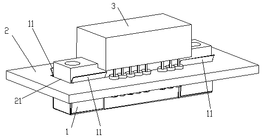
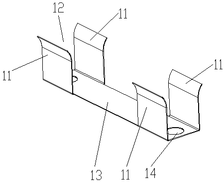
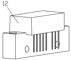
[0052] Such as figure 1 , figure 2 , image 3 with Figure 4 As shown, the grounding device for electronic components includes a PCB board 2 provided with a mounting notch 21 for mounting electronic components 3, and a grounding spring 1 is provided in the mounting notch 21. The inside and outside of the grounding spring 1 are in contact with the electronic components 3 and the PCB board 2 respectively, so that the electronic components 3 are grounded through the grounding spring 1.

[0053] The inner side of the grounding reed of the present invention refers to the side of the grounding reed near the center of the installation slot, and the outer side of the grounding reed refers to the side close to the PCB board, that is, the inner and outer sides of the grounding reed are located on opposite sides, and The side near the center of the mounting slot and the side near the PCB board respectively.

[0054] A mounting slot is opened on the PCB for installing electronic components. ...

Embodiment 2

[0076] This embodiment is applied to the occasion of grounding electronic components.

[0077] Such as figure 1 As shown, when the electronic component grounding device described in Embodiment 1 is used for grounding, the specific grounding method includes the following steps:

[0078] a. Install the ground reed 1 and install the ground reed 1 in the mounting slot 21 so that the ground reed 1 is in contact with the PCB board 2;

[0079] b. Install the electronic component 3, install the electronic component 3 in the ground reed 1 so that the electronic component 3 is in contact with the ground reed 1.

[0080] The order of step a and step b can also be exchanged. After the electronic component 3 is installed in the grounding reed 1, when the grounding reed 1 is installed, the grounding reed 1 and the electronic component 3 are integrally inserted into the mounting slot 21 Inside.

[0081] By adopting the above methods, the electronic components can be smoothly installed in the PCB boar...


PUM


Abstract

The invention relates to the technical field of electrical equipment and in particular to an electronic component grounding device and method. The electronic component grounding device includes a PCBequipped with a mounting notch used for installing an electronic component. A grounding reed is disposed in the mounting notch. The inner side and the outer side of the grounding reed are in contact with the electronic component and the PCB respectively. The mounting notch is disposed on the PCB of the grounding device so that the electronic component is in tight contact with the PCB via the grounding reed. The device and method solve a problem in the prior art that the electronic component mounted on a circuit board is poorly grounded. The electronic component can be easily mounted on the PCB, has a good grounding effect and is ensured in operation and use safety.

Description

Technical field [0001] The invention relates to the technical field of electrical equipment, in particular to a grounding device and a grounding method for electronic components. Background technique [0002] The circuit board is an important carrier of electronic components and one of the important parts of electrical equipment. The circuit board is usually installed and fixed on the chassis during use, so as to work in the enclosed space of the chassis. The circuit board includes multiple functional units, and each functional unit plays its own functional role. Each functional unit is arranged with numerous electronic components. The circuit board is connected to the chassis to realize the grounding function and ensure the safe operation of the circuit board . [0003] In addition to the integrated circuits and electrical components in the circuit board, the rest of the electronic components need to be installed on the circuit board according to the functional needs and use occa...

Claims


Application Information

Patent Timeline
Patent Type & Authority Applications(China)
IPC IPC(8): H01R12/58H01R12/71H01R13/648H01R43/00
Inventor 黄显杰冯亮肖相余罗俊张鳌林
Owner 成都芯通软件有限公司
Why Eureka
Try Eureka