

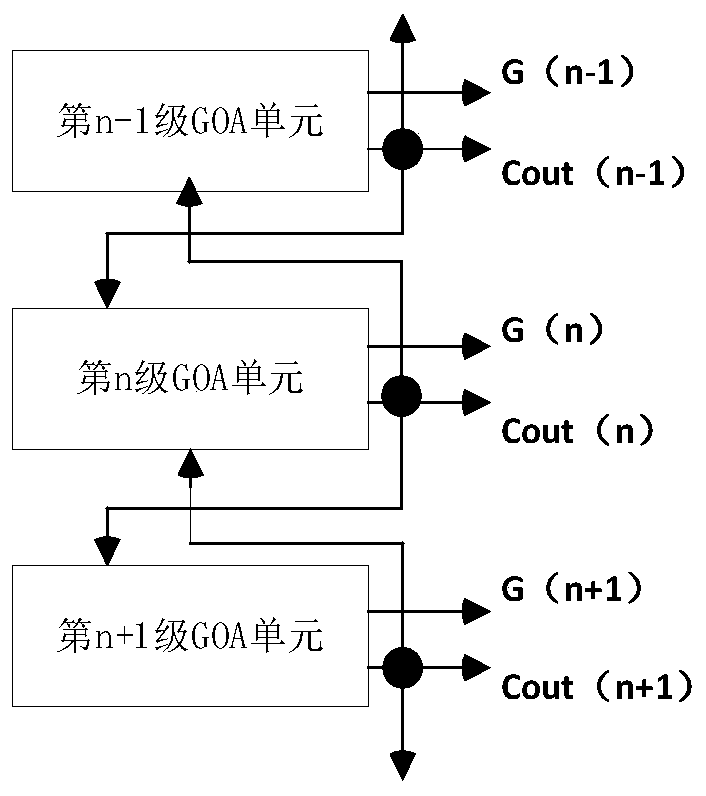
GOA circuit and display panel
A circuit and potential technology, applied in the field of GOA circuit and display panel, can solve the problem of weak output capability of GOA circuit and achieve the effect of improving output capability
- Summary
- Abstract
- Description
- Claims
- Application Information
AI Technical Summary
Problems solved by technology
Method used
Image

Examples
Embodiment Construction
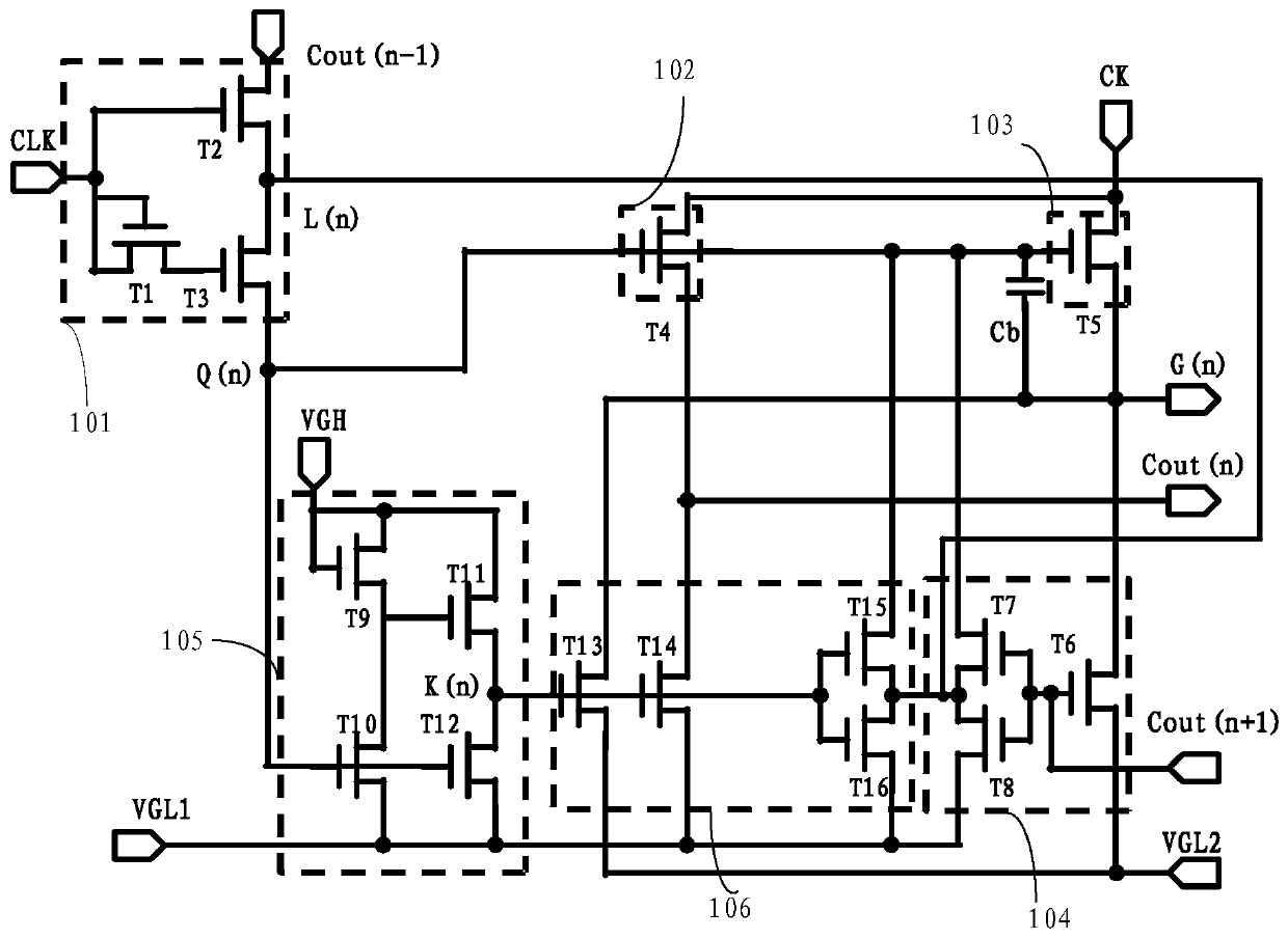
[0035] The technical solutions in the embodiments of the present application will be clearly and completely described below in conjunction with the drawings in the embodiments of the present application. Apparently, the described embodiments are only some of the embodiments of this application, not all of them. Based on the embodiments in this application, all other embodiments obtained by those skilled in the art without making creative efforts belong to the scope of protection of this application.
[0036] The transistors used in all embodiments of this application can be thin film transistors or field effect transistors or other devices with the same characteristics. Since the source and drain of the transistors used here are symmetrical, their source and drain can be interchanged. of. In the embodiment of the present application, in order to distinguish the two poles of the transistor except the gate, one pole is called the source, and the other pole is called the drain. ...
PUM
 Abstract
Description
Claims
Application Information