

A method for cleaning a silicon substrate
A silicon substrate and substrate technology, applied in cleaning methods and appliances, chemical instruments and methods, electrical components, etc., can solve the problems of poor cleaning effect of carbon nanotube root residues, easy to corrode oxide layer, etc., and achieve great promotion value , Excellent spinning performance, highly uniform effect
- Summary
- Abstract
- Description
- Claims
- Application Information
AI Technical Summary
Problems solved by technology
Method used
Image


Examples
Embodiment 1
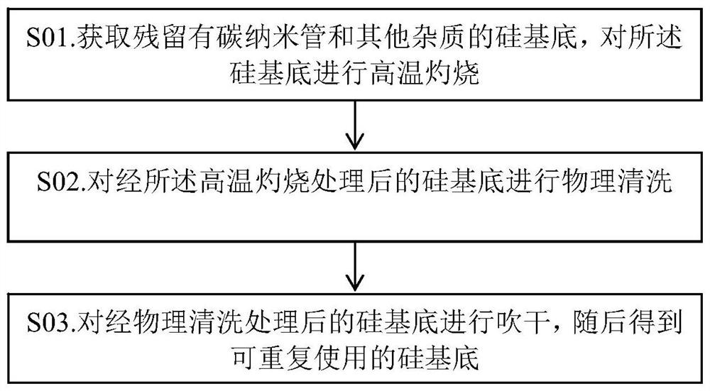
[0054] Obtain 200 8-inch silicon substrates with residual carbon nanotubes and other impurities, and use high-temperature burning for processing. Specifically, the silicon substrate after carbon nanotube growth was placed in an oven, and the high-temperature burning temperature was set to 1450° C., and the burning treatment was performed for 30 minutes. Physically clean the silicon substrate after the high-temperature burning treatment; first wash and rinse with pure water for 4 minutes, and then use a flat-panel cleaning machine to scrub. On the roller of the machine, the silicon wafer is driven forward by the roller, and the front of the silicon wafer contacts the brush head rotating in the same direction as the roller, and the cleaning rate is 1min / piece. The silicon substrate after the physical cleaning treatment is dried, specifically, the drying temperature is 35° C., and the drying wind speed is 2.5 m / s, and then a reusable silicon substrate is obtained.
Embodiment 2
[0056] Obtain 200 8-inch silicon substrates with residual carbon nanotubes and other impurities, and use the first high-temperature burning to process. Specifically, place the silicon substrate after carbon nanotube growth in an oven, set the temperature of the first high-temperature burning to 650° C., and burn for 2 minutes. The silicon substrate burned at the first high temperature is subjected to a second high temperature burning treatment at 1500°C for 20 minutes. Physically clean the silicon substrate after the high-temperature burning treatment; first wash and rinse with pure water for 4 minutes, and then use a flat-panel cleaning machine to scrub. On the roller of the machine, the silicon wafer is driven forward by the roller, and the front of the silicon wafer contacts the brush head rotating in the same direction as the roller, and the cleaning rate is 1min / piece. The silicon substrate after the physical cleaning treatment is dried, specifically, the drying temperat...
Embodiment 3
[0058] Obtain 200 8-inch silicon substrates with residual carbon nanotubes and other impurities, and use the first high-temperature burning to process. Specifically, place the silicon substrate after carbon nanotube growth in an oven, set the temperature of the first high-temperature burning to 650° C., and burn for 2 minutes. The silicon substrate burned at the first high temperature is subjected to a second high temperature burning treatment at 1400°C for 25 minutes. Physically clean the silicon substrate after the high-temperature burning treatment; first wash and rinse with pure water for 4 minutes, and then use a flat-panel cleaning machine to scrub. On the roller of the machine, the silicon wafer is driven forward by the roller, and the front of the silicon wafer contacts the brush head rotating in the same direction as the roller, and the cleaning rate is 1min / piece. The silicon substrate after the physical cleaning treatment is dried, specifically, the drying temperat...
PUM
 Abstract
Description
Claims
Application Information