Hot pressing soldering circuit board and manufacturing method thereof

A manufacturing method and a technology of circuit boards, which are applied in the fields of printed circuit manufacturing, printed circuits, and printed circuits assembled with electrical components, can solve the problems of reduced spacing between pads for hot-press melting soldering, increased short-circuit of pads, etc., and achieve improved Design density, improved thermal conductivity, and lower temperature effects

CN110856375BActive Publication Date: 2021-11-16HONGQISHENG PRECISION ELECTRONICS (QINHUANGDAO) CO LTD +1
0 Cites 0 Cited by

Patent Information

Authority / Receiving Office
CN · China
Patent Type
Patents(China)
Current Assignee / Owner
Publication Date
2021-11-16

Smart Images

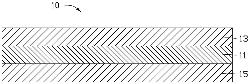
  • Figure 1
    Figure 1
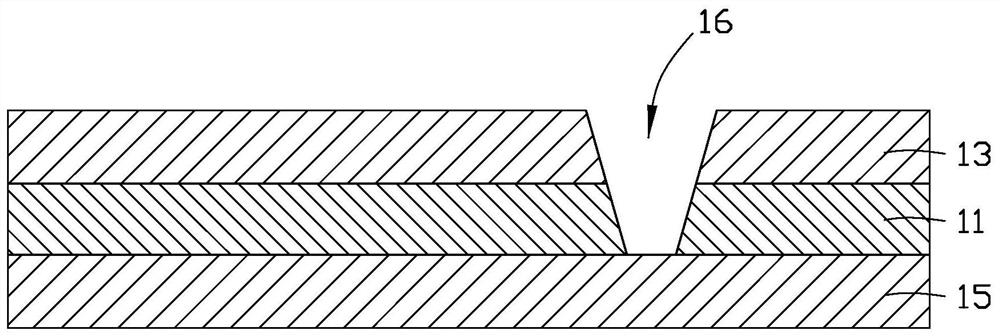
  • Figure 2
    Figure 2
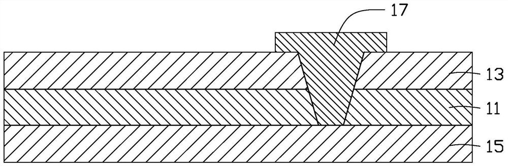
  • Figure 3
    Figure 3
Patent Text Reader

Abstract

A method for manufacturing a circuit board by hot pressing and melting soldering, which includes the following steps: providing a semi-finished product of a flexible circuit board, the semi-finished product of the flexible circuit board includes a first base layer, a first conductive circuit layer and a second copper layer, The first electroplating layer outside the second copper layer, the first conductive circuit layer is electrically connected to the second copper layer; etching the first electroplating layer to obtain at least one step layer; etching the second copper layer to form a second conductive circuit layer to obtain a flexible circuit plate, at least one pad is etched on the second conductive circuit layer relative to at least one step layer, the size of the pad is larger than the size of the step layer to leave space for overflowing tin on both sides of the pad; tin is printed on the step layer paste; and attach the flexible circuit board to another circuit board, and reflow soldering by pulse heating, so that the solder paste is melted and cooled to form a welding layer on the step layer and the welding pad, and the flexible circuit board is fixed and guided to another circuit board. Pass. The invention also provides a circuit board welded by hot pressing and melting tin.
Need to check novelty before this filing date? Find Prior Art

Description

technical field

[0001] The invention relates to a circuit board and a manufacturing method thereof, in particular to a hot-pressing soldering soldering circuit board and a manufacturing method thereof. Background technique

[0002] In recent years, electronic products are widely used in daily work and life, and the demand for miniaturization, multi-function and high performance is getting higher and higher. The density and precision of the board-to-board connection are getting higher and higher. At present, the connection between the board and the board is carried out by the stacking method of hot-press melting tin welding. The principle of hot-press melting soldering is to print the solder paste on the pad of the circuit board first, melt the solder paste and pre-solder it on the circuit board after going through the reflow oven, and then place the object to be soldered on the solder paste already printed Then use the heat of the thermal head to melt the solder and connec...

Examples

Embodiment Construction

[0025] The following will clearly and completely describe the technical solutions in the embodiments of the present invention with reference to the accompanying drawings in the embodiments of the present invention. Obviously, the described embodiments are only some, not all, embodiments of the present invention. Based on the embodiments of the present invention, all other embodiments obtained by persons of ordinary skill in the art without making creative efforts belong to the protection scope of the present invention.

[0026] Unless otherwise defined, all technical and scientific terms used herein have the same meaning as commonly understood by one of ordinary skill in the technical field of the invention. The terms used herein in the description of the present invention are for the purpose of describing specific embodiments only, and are not intended to limit the present invention.

[0027] Some embodiments of the present invention will be described in detail below in conju...