Square flat pin-free packaging structure, preparation method thereof and electronic device

A leadless packaging, square and flat technology, applied in the direction of electric solid devices, electrical components, semiconductor devices, etc., can solve the problems of insufficient quantity and the impact of integration, and achieve the effect of increasing pin density and packaging integration

Inactive Publication Date: 2020-06-12
QINGDAO GOERTEK MICROELECTRONICS RES INST CO LTD
View PDF3 Cites 5 Cited by
  • Summary
  • Abstract
  • Description
  • Claims
  • Application Information

AI Technical Summary

Problems solved by technology

However, QFN is currently limited by the insufficient number of I / O (input / output, input and output pins), so the integration level is also affected accordingly.

Method used


Image

  • Square flat pin-free packaging structure, preparation method thereof and electronic device
  • Square flat pin-free packaging structure, preparation method thereof and electronic device
  • Square flat pin-free packaging structure, preparation method thereof and electronic device

Examples


Embodiment Construction

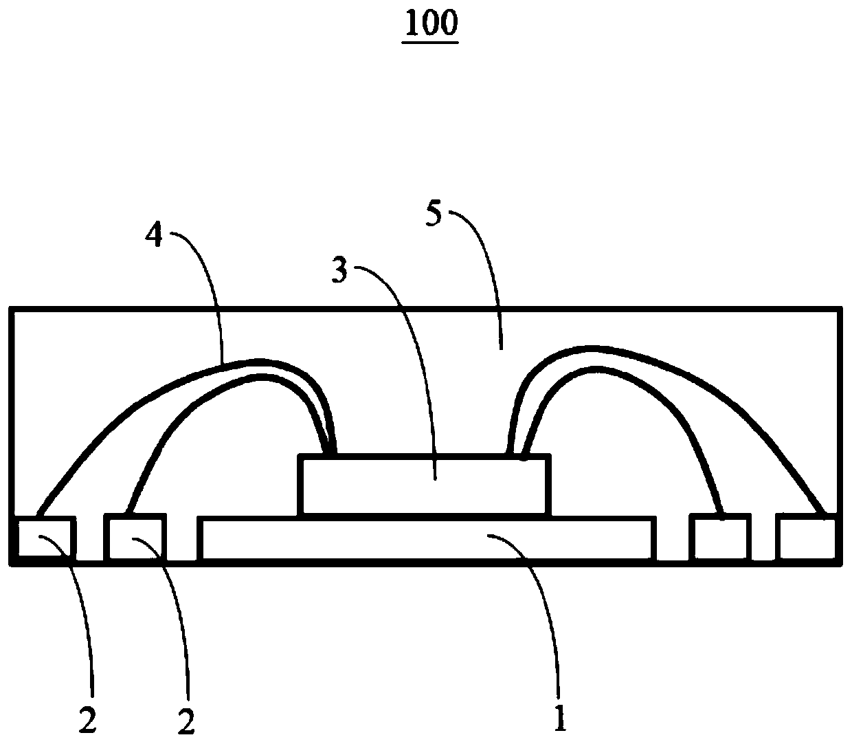
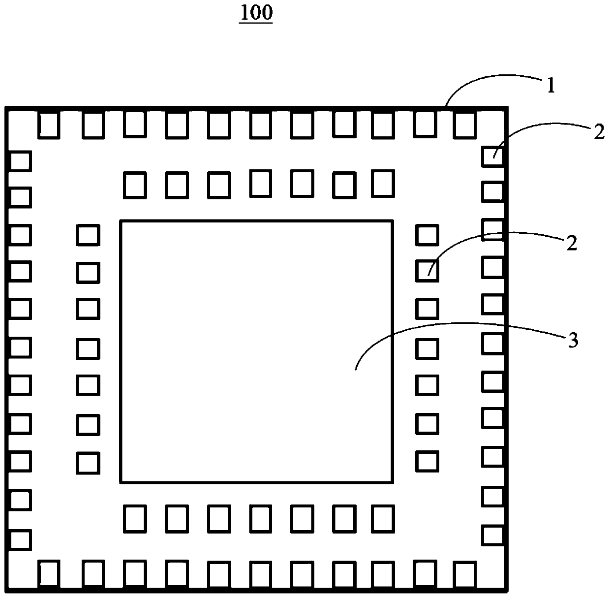
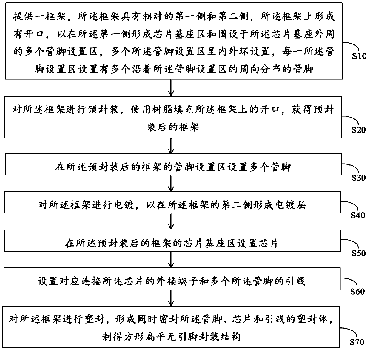
[0042] In order to make the purpose, technical solutions and advantages of the embodiments of the present invention clearer, the technical solutions in the embodiments of the present invention will be clearly and completely described below. Those who do not indicate the specific conditions in the examples are carried out according to the conventional conditions or the conditions suggested by the manufacturer. The reagents or instruments used were not indicated by the manufacturer, and they were all conventional products that could be purchased from the market. In addition, the meaning of "and / or" appearing in the whole text includes three parallel schemes, taking "A and / or B" as an example, including scheme A, scheme B, or schemes that both A and B satisfy. In addition, the technical solutions of various embodiments can be combined with each other, but it must be based on the realization of those skilled in the art. When the combination of technical solutions is contradictory ...


PUM


Abstract

The invention discloses a square flat pin-free packaging structure, a preparation method thereof and an electronic device. The square flat pin-free packaging structure comprises a frame, a chip, leadsand a plastic packaging body, wherein the frame is provided with a first side and a second side which are opposite to each other, the first side is provided with a chip base and a plurality of pin setting areas arranged at the periphery of the chip base in a surrounding manner, the plurality of pin setting areas are arranged in an inner and outer ring manner, and each pin setting area is providedwith a plurality of pins distributed along the circumferential direction of the pin setting area; wherein the chip is arranged on the chip base; the pin is correspondingly connected with an externalterminal of the chip and the plurality of pins; the plastic package body is arranged on the frame and seals the pins, the chip and the pins at the same time. According to the invention, the pluralityof pin groups arranged in the inner and outer rings are arranged around the chip, so that the pin density of the square flat pin-free packaging structure is improved, and the improvement of the packaging integration level is facilitated.

Description

technical field [0001] The invention relates to the technical field of square flat leadless package structure, in particular to a square flat leadless package structure, a preparation method thereof, and an electronic device. Background technique [0002] QFN (Quad Flat Non-leaded Package, Quad Flat Non-leaded Package) is a common package form, which has good electrical and thermal performance, small size, light weight, low development cost, and its application is very wide. However, the current QFN is limited by the insufficient number of I / O (input / output, input and output pins), so the integration degree is also affected accordingly. Contents of the invention [0003] The main purpose of the present invention is to provide a square flat no-lead packaging structure and its preparation method, as well as an electronic device, aiming at increasing the pin density of the square flat no-lead packaging structure. [0004] In order to achieve the above object, the present inv...

Claims


Application Information

Patent Timeline
Patent Type & Authority Applications(China)
IPC IPC(8): H01L23/495H01L21/56H01L21/60
CPCH01L21/56H01L23/49503H01L23/49517H01L24/85H01L2224/48091H01L2224/48247H01L2224/73265H01L2224/97H01L2924/181H01L2924/00012H01L2924/00014
Inventor 尹保冠于上家陈建超
Owner QINGDAO GOERTEK MICROELECTRONICS RES INST CO LTD
Why Eureka
Try Eureka