Conductive adhesive structure and display device

A display device and conductive adhesive technology, applied to the conductive layer, conductor, circuit, etc. on the insulating carrier, can solve the problems of darkening of the fingerprint hole area, affecting the TFT characteristics of the display panel, and uneven display brightness.

Active Publication Date: 2020-07-14
BOE TECH GRP CO LTD +1
View PDF5 Cites 4 Cited by
  • Summary
  • Abstract
  • Description
  • Claims
  • Application Information

AI Technical Summary

Problems solved by technology

However, as the area of ​​the fingerprint unlocking area expands, it will inevitably increase the window area of ​​the heat dissipation film on the back of the OLED panel and expose a large area of ​​U-film (protective film), and the surface impedance of U-film itself is so large that it is almost non-conductive. Generally, the induced charge accumulation generated on the surface will react against

Method used


Image

  • Conductive adhesive structure and display device
  • Conductive adhesive structure and display device
  • Conductive adhesive structure and display device

Examples


Example Embodiment

[0022] The following will clearly and completely describe the technical solutions in the embodiments of the present invention with reference to the accompanying drawings in the embodiments of the present invention. Obviously, the described embodiments are only some, not all, embodiments of the present invention. Based on the embodiments of the present invention, all other embodiments obtained by persons of ordinary skill in the art without making creative efforts belong to the protection scope of the present invention.

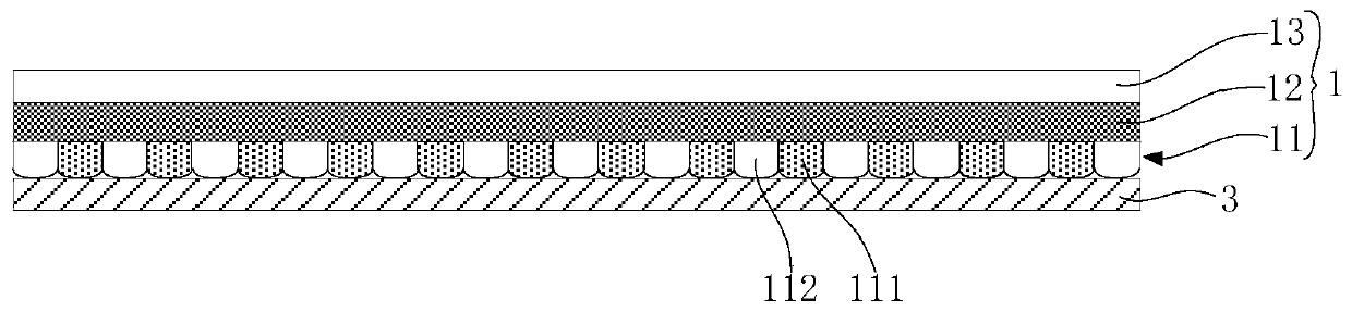
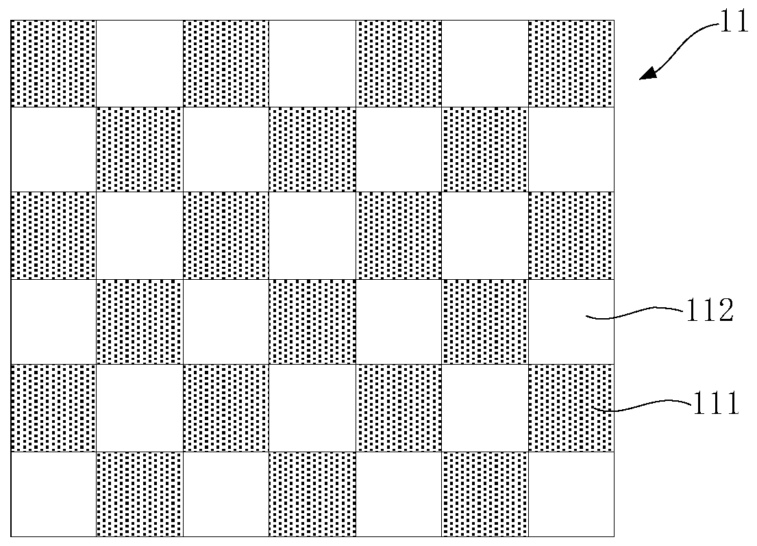
[0023] like figure 1 , figure 2 and image 3 As shown, a conductive adhesive structure 1 includes: a first adhesive layer 11, a conductive layer 12 and a second adhesive layer 13 that are stacked in sequence, and the first adhesive layer 11 is provided with a plurality of conductive particle filling regions 111 distributed at intervals , the conductive particle filled region 111 is provided with conductive particles, and the conductive particles are electri...


PUM


Abstract

The invention relates to the technical field of display, and discloses a conductive adhesive structure and a display device. The conductive adhesive structure comprises a first adhesive layer, a conductive layer and a second adhesive layer which are sequentially arranged in a stacked mode, a plurality of conductive particle filling areas distributed at intervals are arranged in the first adhesivelayer, conductive particles are arranged in the conductive particle filling areas, and the conductive particles are electrically connected with the conductive layer. Based on the conductive adhesive structure, display panel backside, inductive charges generated on the back face of the display panel can be guided and dispersed evenly in the whole face of the back face of the display panel, the situation that the inductive charges are gathered is avoided, the problem that a fingerprint unlocking area becomes dark is solved, it is guaranteed that the display brightness of the unlocking area is uniform and consistent with that of other display areas, and the overall brightness of the display panel is displayed evenly.

Description

technical field [0001] The invention relates to the field of display technology, in particular to a conductive adhesive structure and a display device. Background technique [0002] At present, in order to meet the ever-changing technological needs of consumers, more and more new technologies are gradually applied to mobile phone display modules, among which the large fingerprint unlocking area and even half-screen and full-screen fingerprint unlocking areas are the key link. However, as the area of ​​the fingerprint unlocking area expands, it will inevitably increase the window area of ​​the heat dissipation film on the back of the OLED panel and expose a large area of ​​U-film (protective film), and the surface impedance of U-film itself is so large that it is almost non-conductive. Generally, the induced charge accumulation generated on the surface will react against the Panel and affect the TFT characteristics of the display panel. Therefore, the fingerprint hole Mura ph...

Claims


Application Information

Patent Timeline
IPC IPC(8): B32B15/20B32B15/08B32B27/00B32B27/06B32B3/12B32B3/08B32B33/00H01B5/14H01B5/16
CPCB32B15/20B32B15/046B32B5/18B32B3/12B32B3/085B32B33/00H01B5/14H01B5/16B32B2266/0214B32B2307/202B32B2307/206B32B2307/302B32B2457/20
Inventor 王梓鉴陆旭谢涛峰王志强刘莉李飞
Owner BOE TECH GRP CO LTD
Why Eureka
Try Eureka