Unified binary phase modulating and demodulating method

A modulation and demodulation, binary phase technology, applied in the field of digital information transmission

CN1889550AInactive Publication Date: 2007-01-03SOUTHEAST UNIV
1 Cites 21 Cited by

Patent Information

Authority / Receiving Office
CN · China
Current Assignee / Owner
Publication Date
2007-01-03
Estimated Expiration
Not applicable · inactive patent

Smart Images

  • Figure 1
    Figure 1
  • Figure 2
    Figure 2
  • Figure 3
    Figure 3
Patent Text Reader

Abstract

A information modulating and demodulating method used on digital communication includes realizing modulation by utilizing binary information code element to directly vary abrupt phase of sine carrier wave, utilizing lock phase ring to realize demodulation, making modulated signal g0(t) corresponding to number zero be sine wave of N carrier wave period and making g1(t) corresponding to number one be in sine wave of N carrier wave period with frequency of fc, applying phase jump off angle theta and parameter tau as modulation index for varying signal bandwidth and transmission code rate as well as demodulation property.
Need to check novelty before this filing date? Find Prior Art

Description

technical field

[0001] The invention relates to an information modulation and demodulation method for digital communication, belonging to the technical field of digital information transmission. Background technique

[0002] In a digital communication system, the process of moving the baseband signal representing binary data up to a given transmission frequency band is called modulation, and the opposite process is called demodulation. In practice, we not only pursue the highest possible frequency band utilization, that is, transmit a higher digital rate (measured in bps / Hz) within the unit frequency band; we also hope to use the transmission energy more effectively to obtain better transmission effects .

[0003] The traditional binary phase shift keying (BPSK) modulation achieves the conversion of logic "0" and "1" by inverting the sinusoidal carrier at its zero phase at θ=180°, where the sine wave representing "0" and The inverted sine wave representing "1" lasts for th...

Examples

Embodiment Construction

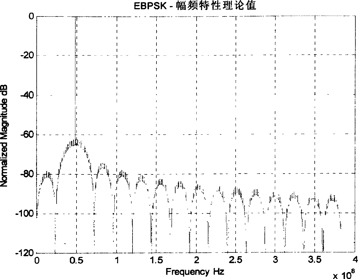
[0041] Take θ=π / 4, f c =48MHz, get the power spectrum of the EBPSK modulation signal as figure 1 Shown, where the ordinate is the power spectrum amplitude at the carrier frequency as 0dB. It can be seen from the figure that the energy of the EBPSK modulation signal is highly concentrated, and the carrier frequency amplitude is at least 60dB (1 million times) higher than other sidebands. The time domain waveform of the EBPSK modulation signal is indeed very similar to a sine wave.

[0042] This method uses binary information symbols to directly change the sudden phase of the sinusoidal carrier to realize modulation, and uses a phase-locked loop to realize demodulation, so that the modulated signal corresponding to the digital "0" g 0 (t) is a sine wave of N carrier periods, and g corresponding to the number "1" 1 (t) is at frequency f c In the sine wave of N carrier periods of , the phase jump of the first K periods has an angle of θ; that is

[0043] f 0...