Interface converting circuit

Active Publication Date: 2009-02-12
ALPHA NETWORKS INC
View PDF6 Cites 9 Cited by
  • Summary
  • Abstract
  • Description
  • Claims
  • Application Information

AI Technical Summary

Benefits of technology

[0010]The present invention provides an interface converting circuit, applied between a 3D de-interlace chip and a rear-end image compression chip, comprising: a reducing FPS circuit, for dividing a first vertical synchronization signal to generate a second vertical synchronization signal, and converting a first horizontal synchronization signal to a second horizontal synchronization signal by masking the first horizontal synchronization signal according to the second vertical synchronization signal; a pixel clock multiplier, for multiplying a first pixel

Problems solved by technology

However, if the object depicted in FIG. 2 is moving at a relatively high speed and is captured by the image-capturing m

Method used


Image

  • Interface converting circuit
  • Interface converting circuit
  • Interface converting circuit

Examples


Embodiment Construction

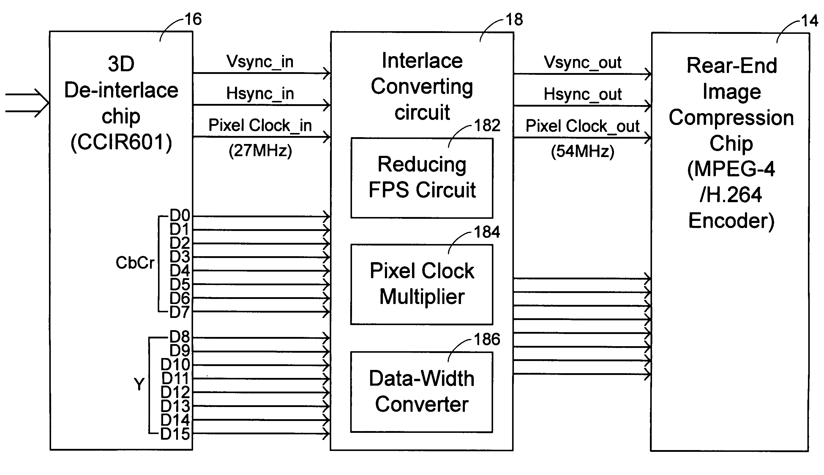
[0027]FIG. 5 is a block diagram showing an image processing system. The image processing system comprises: a 3D de-interlace chip 16 (CCIR601 specification), a rear-end image compression chip 14 (i.e., MPEG-4 / H.264 encoder), and an interface converting circuit 18 of the present invention. The interface converting circuit 18 further comprises: a reducing FPS circuit 182, a pixel clock multiplier 184, and a data-width converter 186.

[0028]As depicted in FIG. 5, after the 3D de-interlace chip 16 receiving the odd-field signal and the even-field signal derived from the image-capturing module 10 with a frame rate of 30 frames per second (30 FPS), the 3D de-interlace chip 16 then generates frames with a frame rate of 60 frames per second (60 FPS) through executing the dynamic prediction compensation to each odd-filed signal and each even-field signal, these frames, constituted by Y, Cb, Cr signals, are further transmitted to the interface converting circuit 18 of the present invention with...


PUM


Abstract

An interface converting circuit applied between a 3D de-interlace chip and a rear-end image compression chip. The interface converting circuit includes: a reducing FPS circuit, for dividing a first vertical synchronization signal to generate a second vertical synchronization signal, and converting a first horizontal synchronization signal to a second horizontal synchronization signal by masking the first horizontal synchronization signal according to the second vertical synchronization signal; a pixel clock multiplier, for multiplying a first pixel clock signal to generate a second pixel clock signal; and, a data-width converter, for converting an input signal with M bits data width, which is transmitted at a frequency of the first pixel clock signal by the 3D de-interlace chip, to an output signal with M/2 bits data width, which is transmitted at a frequency of the second pixel clock signal.

Description

FIELD OF THE INVENTION[0001]The present invention relates to an interface converting circuit, and more particularly to an interface converting circuit applied between a 3D de-interlace chip and a rear-end image compression chip.BACKGROUND OF THE INVENTION[0002]FIG. 1 is a block diagram showing a conventional image processing system of an IP CAM. The IP CAM image processing system comprises: an image-capturing module 10 and a rear-end image compression chip 14. The image-capturing module 10 further comprises a charge coupled device (CCD) and a digital signal processor (not shown).[0003]When the CCD of the image-capturing module 10 is capturing an object, the capturing signals, generated by the CCD, is transmitted to the digital signal processor. The capturing signals are then transferred to pixel-format signals (i.e., resolution 720×480) by the digital signal processor. The digital signal processor then sequentially outputs an odd-field signal (resolution 720×240) and an even-field s...

Claims


Application Information

Patent Timeline
IPC IPC(8): H04N7/01H04N19/00H04N19/70H04N19/85
CPCH04N5/217H04N7/012H04N5/335H04N23/81H04N25/00
InventorLO, CHUNG-MING
OwnerALPHA NETWORKS INC