
Monitoring marking layout for microlens baking process
A microlens and layout technology, which is applied to lenses, photolithography process exposure devices, microlithography exposure equipment, etc., can solve the problem of inability to evaluate the flow of photoresist. The quality of the microlens array, poor efficiency, and difficulty in reflective patterns And other issues
Patent Information
- Authority / Receiving Office
- CN · China
- Patent Type
- Patents(China)
- Current Assignee / Owner
- Publication Date
- 2008-03-05
Smart Images
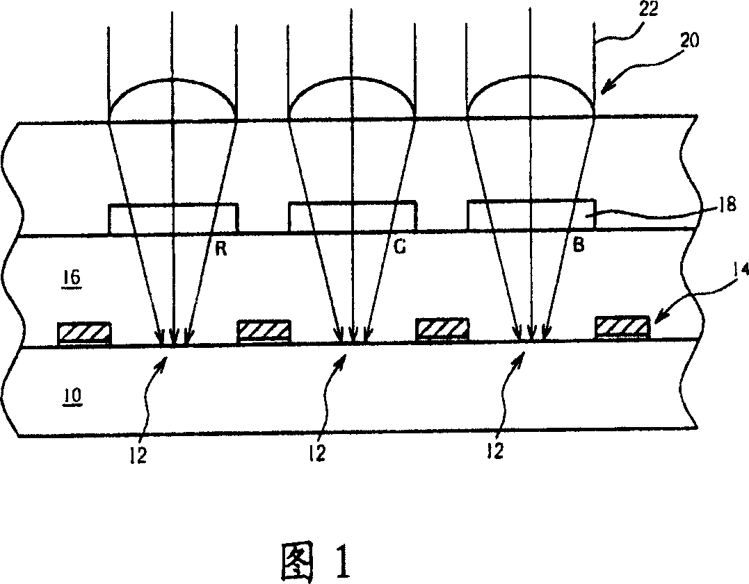
Figure 1 
Figure 2 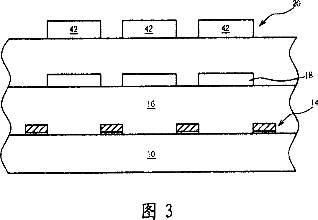
Figure 3
Abstract
Description
technical field
[0001] The invention relates to the manufacture of microlenses, in particular to a monitoring mark for the baking process of the microlenses, which is made on the cutting line and can be used to evaluate whether the microlens array has been baked and the quality of the baking. Background technique
[0002] As known to those in the industry, microlens technology has been widely used in many optoelectronic products currently on the market, such as digital cameras and digital video cameras. The purpose of using the microlens is to control the direction of the light, so that the light can be gathered in the sensing area of the light sensing chip.
[0003] A digital camera usually includes a stacked color filter array (CFA) and a charge-coupled device (CCD) or complementary metal oxide semiconductor (CMOS) image sensor, wherein the color filter array includes three (R / G / B or above staggered filter channels, each filter channel only allows light of a specific f...
Examples
Embodiment Construction
[0032] Please refer to FIG. 5 , which shows the layout of the monitoring marks and the top view of the microlens array for checking the baked state of the microlenses according to the preferred embodiment of the present invention. As shown in FIG. 5 , the microlens array 20 is formed in the active circuit area 101 with a plurality of unbaked photoresist blocks 42 . In the present invention, the monitoring mark layout 100 for checking the baked state of the microlens can be formed in the scribe area 102 and defined simultaneously with the photoresist block 42 . The size of the layout shown in the figure is for reference only.
[0033] According to this preferred embodiment, the monitoring mark layout 100 for checking the baked state of the microlens can be a U-shaped pattern, including two vertical line patterns 110 and 120 arranged in parallel to each other, and a horizontal line pattern 130 connecting the aforementioned two vertical lines. Line patterns 110 and 120 . The ver...