
Preparation method for complementary metal oxide semiconductor element with dual metal grid
An oxide semiconductor and double metal gate technology, which is applied in the field of complementary metal oxide semiconductor components, can solve the problems of complex integration technology and process control, and strict requirements for material thickness and composition control.
Patent Information
- Authority / Receiving Office
- CN · China
- Patent Type
- Patents(China)
- Current Assignee / Owner
- Publication Date
- 2012-09-19
Smart Images
Figure 1 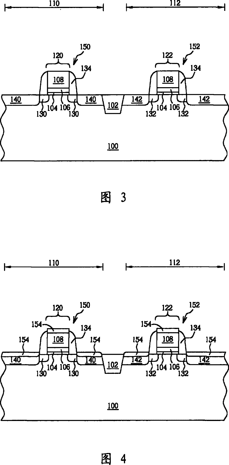
Figure 2 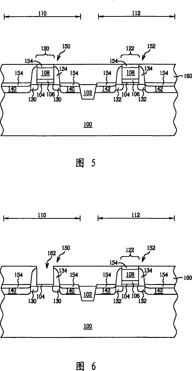
Figure 3
Abstract
Description
technical field
[0001] The present invention relates to a manufacturing method of a complementary metal-oxide semiconductor (hereinafter referred to as CMOS) element with a dual metal gate, especially a gate last ) process with a double metal gate CMOS element manufacturing method. Background technique
[0002] As the size of CMOS devices continues to shrink, the traditional method of reducing the gate dielectric layer, such as reducing the thickness of the silicon dioxide layer, to achieve the purpose of optimization, is facing problems caused by the tunneling effect of electrons. Physical limitation of excessive leakage current. In order to effectively extend the generation evolution of logic elements, high dielectric constant (hereinafter referred to as High-K) materials can effectively reduce the physical limit thickness, and at the same equivalent oxide thickness (equivalent oxide thickness, hereinafter referred to as EOT) Under the advantages of effectively reducing ...
Examples
Embodiment Construction
[0041] see Figure 2 to Figure 8 , Figure 2 to Figure 8 It is a schematic diagram of the first preferred embodiment of the method for manufacturing a CMOS device with a double metal gate provided by the present invention. Such as figure 2As shown, a substrate 100 is firstly provided, such as a silicon substrate, a silicon-containing substrate, or a silicon-on-insulator (hereinafter referred to as SOI) substrate, etc., and a first active region 110 and a second active region 110 are defined on the surface of the substrate 100. The active region 112 , and a shallow trench isolation (STI) 102 for electrically isolating the first active region 110 and the second active region 112 is formed in the substrate 100 . Next, a high dielectric constant (hereinafter referred to as High-K) gate dielectric layer 104 , a tantalum carbide (TaC) layer 106 , and a polysilicon layer 108 are sequentially formed on the substrate 100 . In addition, in the first embodiment, a protection layer (n...