
Method for manufacturing solar thin film light transmitting component
A technology for thin-film solar energy and light-transmitting components, which is applied in the manufacturing of electrical components, semiconductor devices, and final products, etc., can solve problems such as affecting the efficiency and yield of components, unfavorable industrial production, and reducing component performance, so as to improve efficiency and satisfy Market demand, the effect of reducing defects
Patent Information
- Authority / Receiving Office
- CN · China
- Patent Type
- Applications(China)
- Current Assignee / Owner
- Publication Date
- 2012-03-14
- Estimated Expiration
- Not applicable · inactive patent
Smart Images
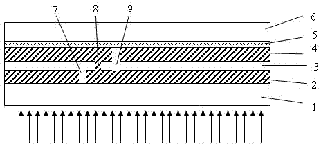
Figure 1 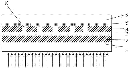
Figure 2 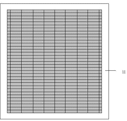
Figure 3
Abstract
Description
technical field
[0001] The invention relates to a method for preparing a thin-film solar light-transmitting component, which belongs to the technical field of photovoltaic applications. Background technique
[0002] At present, photovoltaic integrated buildings are the most advanced and potential high-tech green energy-saving buildings, and it is also one of the important directions for large-scale utilization of photovoltaic technology in the world. Building Integrated Photovoltaics (BIPV) refers to the installation of solar photovoltaic power generation arrays on the outer surface of the maintenance structure of the building to provide electricity. Since the combination of photovoltaic arrays and buildings does not occupy additional ground space, it is the best installation method for photovoltaic power generation systems to be widely used in cities, and thus has attracted much attention. According to the different combination forms of photovoltaic modules and buildings, ...
Examples
Embodiment Construction
[0012] The present invention will be further described through the embodiments below in conjunction with the accompanying drawings.
[0013] This embodiment is a silicon thin film solar cell, and the specific implementation method is:
[0014] 1. Use ultra-clear float glass as the front transparent insulating substrate 1, and use low-pressure chemical vapor deposition technology or magnetron sputtering technology to deposit the front transparent conductive film 2 on the above-mentioned front transparent insulating substrate 1, as the front conductive electrode of the battery ;
[0015] 2. Use a 355nm or 1064nm laser to perform the first laser scribing 7 (Patten1) on the transparent conductive film 2 to realize the insulation between small areas, and use the above-mentioned laser to scribe P1 insulating lines around the edge of the component;
[0016] 3. Prepare an amorphous silicon semiconductor film layer 3 as a photoelectric conversion layer on the above-mentioned front tra...