

Double-polysilicon SOI (Silicon On Insulator) SiGe HBT (Heterojunction Bipolar Transistor) integrated device based on self-aligned technology and preparation method thereof
A technology of self-alignment technology and integrated devices, which is applied in semiconductor/solid-state device manufacturing, electric solid-state devices, semiconductor devices, etc., and can solve problems such as lack of wide application and development, incompatibility of Si technology, and complexity of preparation technology compared with Si technology.
Patent Information
- Authority / Receiving Office
- CN · China
- Patent Type
- Applications(China)
- Current Assignee / Owner
- Publication Date
- 2012-10-17
- Estimated Expiration
- Not applicable · inactive patent
Smart Images
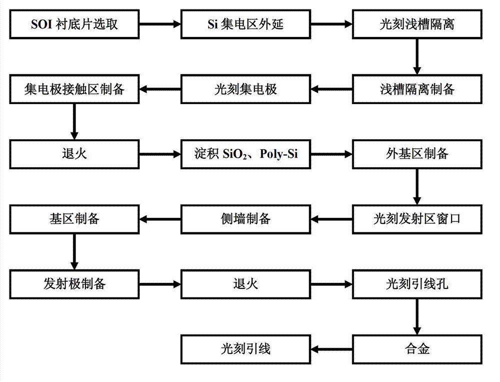
Figure 1 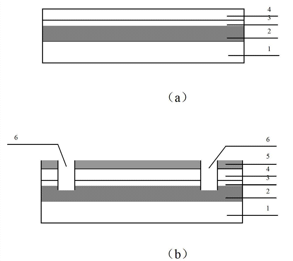
Figure 2 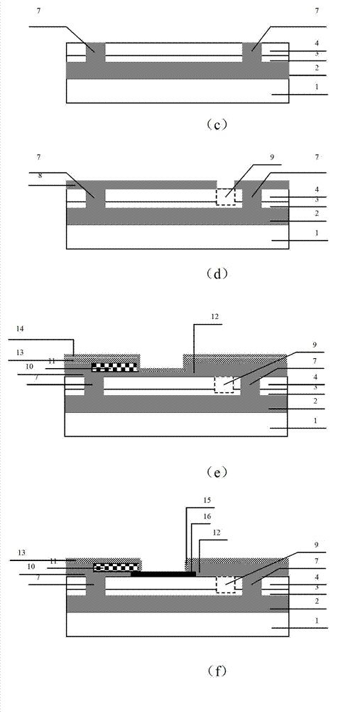
Figure 3
Abstract
Description
Technical field
[0001] The invention belongs to the technical field of semiconductor integrated circuits, and in particular relates to a dual polycrystalline SOI SiGe HBT integrated device based on a self-aligned process and a preparation method. Background technique
[0002] Integrated circuits are the cornerstone and core of the economic development of the information society. As the U.S. engineering technology community recently mentioned the fifth electronic technology among the 20 greatest engineering achievements in the world in the 20th century, “from vacuum tubes to semiconductors and integrated circuits, it has become the cornerstone of intelligent work in various industries today.” One of the typical products that best reflects the characteristics of the knowledge economy. At present, the electronic information industry based on integrated circuits has become the world's largest industry. With the development of integrated circuit technology, the clear boundaries betw...
Examples
Embodiment 1
[0075] Embodiment 1: Provides a method for preparing a dual polycrystalline SOI SiGe HBT integrated device and circuit with a base thickness of 20 nm by using a self-aligned process, the specific steps are as follows:
[0076] Step 1, epitaxial growth, such as figure 2 (A) Shown.
[0077] (1a) Select SOI substrate, the support material 1 of the substrate is Si, and the intermediate layer 2 is SiO 2 , The thickness is 150nm, the upper material 3 is doped with a concentration of 1×10 16 cm -3 N-type Si with a thickness of 100nm;
[0078] (1b) Using chemical vapor deposition (CVD) method, at 600℃, grow a layer of N-type epitaxial Si layer 4 with a thickness of 50nm on the upper layer of Si material as a collector area, the doping concentration of this layer is 1 ×10 16 cm -3 .
[0079] Step 2, shallow trench isolation preparation, such as figure 2 (B) and (c).
[0080] (2a) Using chemical vapor deposition (CVD), at 600℃, deposit a layer of SiO with a thickness of 300nm on the surface ...
Embodiment 2
[0109] Embodiment 2: A method for preparing a dual polycrystalline SOI SiGeHBT integrated device and circuit with a base region thickness of 40 nm using a self-aligned process is provided. The specific steps are as follows:
[0110] Step 1, epitaxial growth, such as figure 2 (A) Shown.
[0111] (1a) Select an SOI substrate, the lower support material 1 of the substrate is Si, and the intermediate layer 2 is SiO 2 , The thickness is 300nm, the upper material 3 is doped with a concentration of 5×10 16 cm -3 N-type Si with a thickness of 120nm;
[0112] (1b) Using the chemical vapor deposition (CVD) method, at 700℃, grow a layer of N-type epitaxial Si layer 4 with a thickness of 80nm on the upper Si material as a collector area, the doping concentration of this layer is 5 ×10 16 cm -3 .
[0113] Step 2, shallow trench isolation preparation, such as figure 2 (B) and (c).
[0114] (2a) Using chemical vapor deposition (CVD) method, at 700℃, deposit a layer of SiO with a thickness of 400n...
Embodiment 3
[0143] Embodiment 3: Provides a method for preparing a dual polycrystalline SOI SiGeHBT integrated device and circuit with a base region thickness of 60 nm by using a self-aligned process, the specific steps are as follows:
[0144] Step 1, epitaxial growth, such as figure 2 (A) Shown.
[0145] (1a) Select an SOI substrate, the lower support material 1 of the substrate is Si, and the intermediate layer 2 is SiO 2 , The thickness is 400nm, and the upper material 3 is doped with a concentration of 1×10 17 cm -3 N-type Si with a thickness of 150nm;
[0146] (1b) Using the chemical vapor deposition (CVD) method, at 750℃, grow a layer of N-type epitaxial Si layer 4 with a thickness of 100nm on the upper Si material as a collector area, the doping concentration of this layer is 1 ×10 17 cm -3 .
[0147] Step 2, shallow trench isolation preparation, such as figure 2 (B) and (c).
[0148] (2a) Using chemical vapor deposition (CVD), at 800℃, deposit a layer of SiO with a thickness of 500nm ...