
Super-junction schottky diode
a super-junction, schottky diode technology, applied in the direction of semiconductor devices, basic electric elements, electrical apparatus, etc., can solve the problems of large forward voltage and reverse recovery time of schottky diodes, large reverse leakage current and poor temperature characteristics, and increase of forward conduction loss, etc., to achieve a smaller forward voltage, better reverse breakdown characteristic, and large forward current
Patent Information
- Authority / Receiving Office
- US · United States
- Patent Type
- Applications(United States)
- Current Assignee / Owner
- Publication Date
- 2018-01-25
- Estimated Expiration
- Not applicable · inactive patent
Smart Images
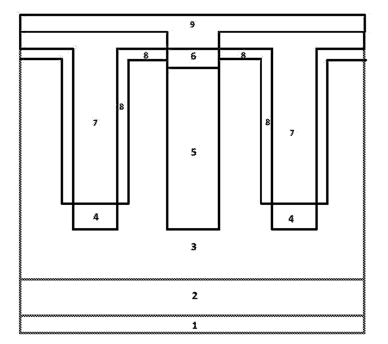
Figure 1 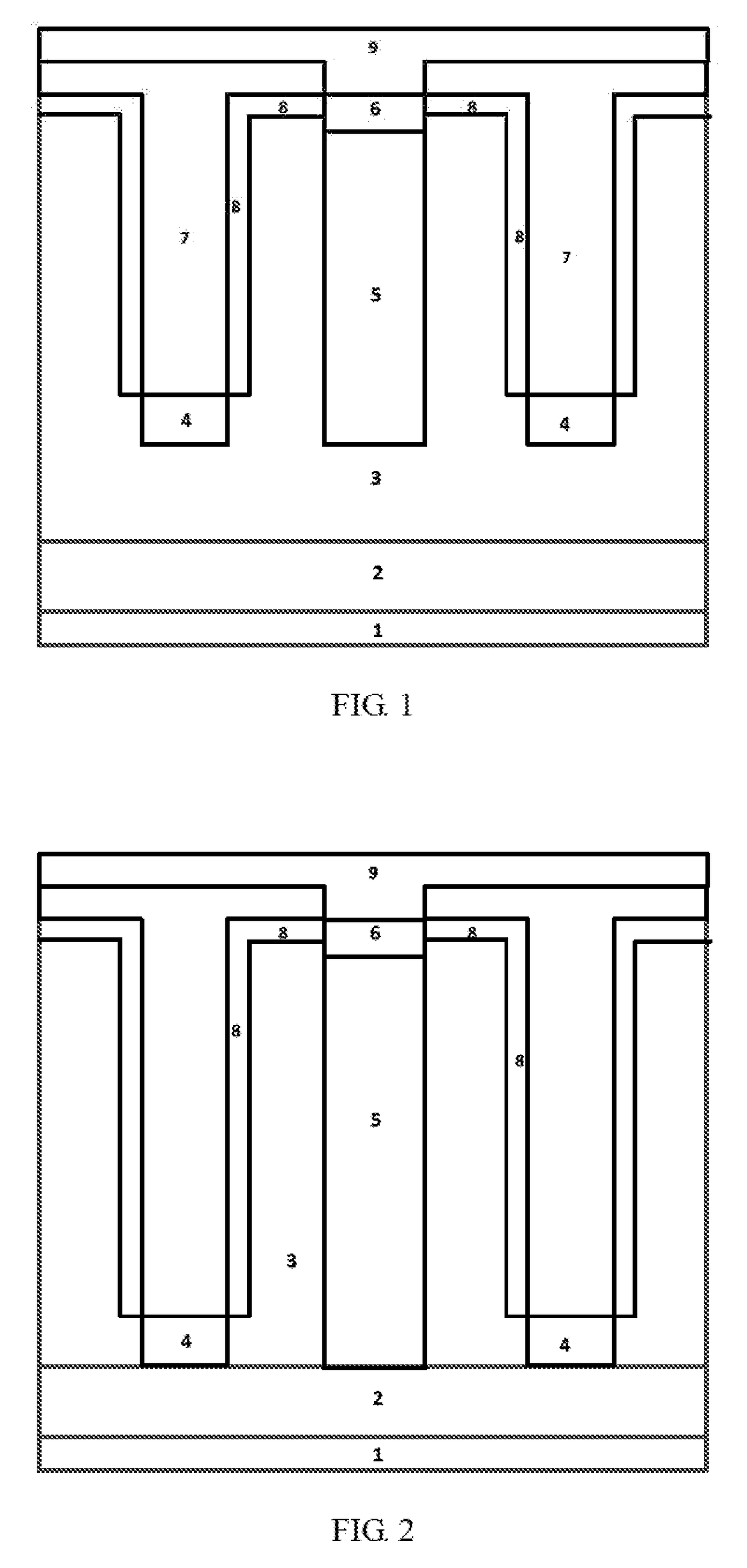
Figure 2 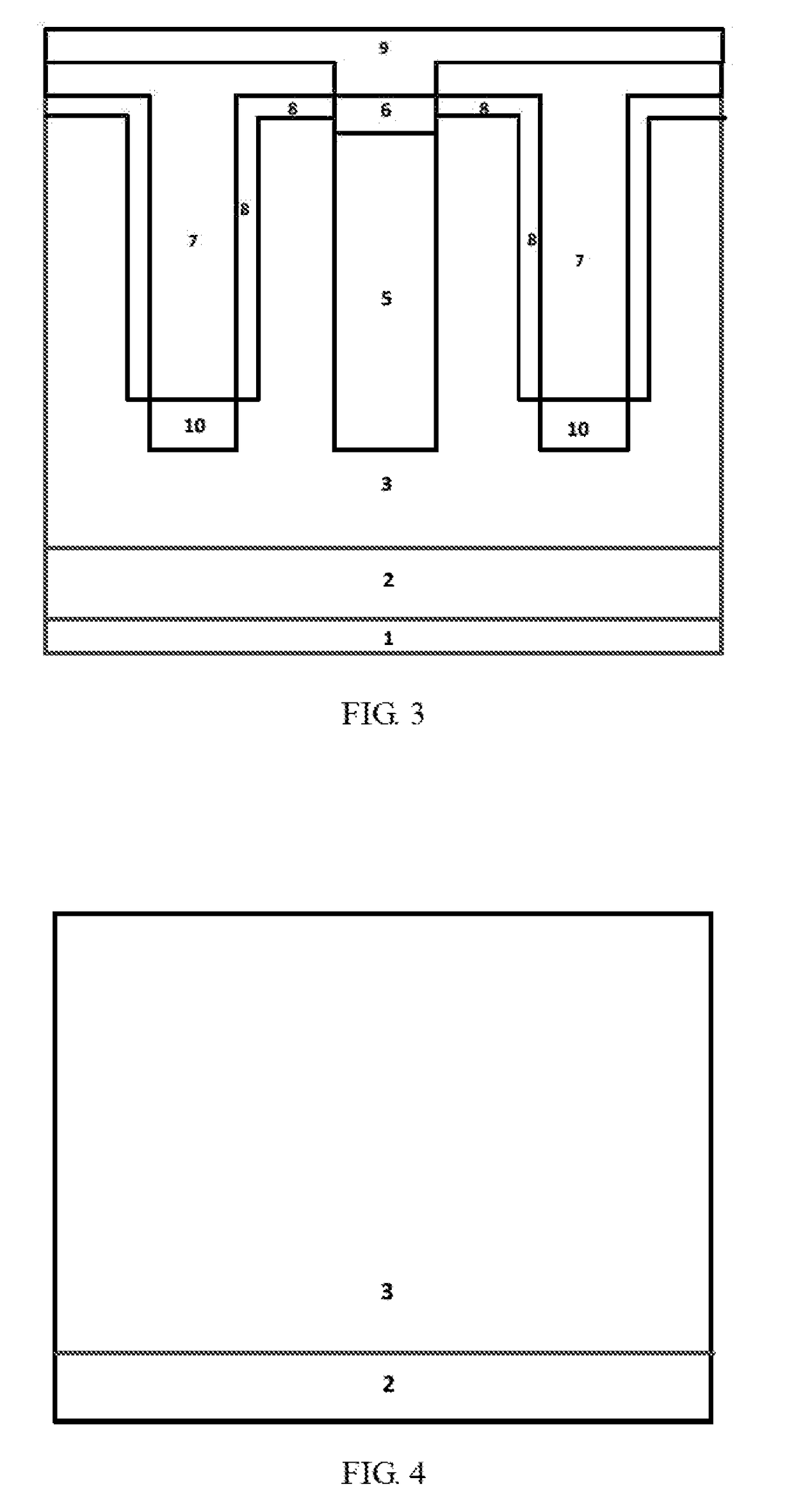
Figure 3
Abstract
Description
[0001] The present application is based on, and claims priority from, Chinese application number 201610596069.4, filed on Jul. 25, 2016, the disclosure of which is hereby incorporated by reference herein in its entirety.TECHNICAL FIELD OF THE INVENTION
[0002] The present invention relates to the technical field of semiconductor devices, particularly to a super-junction schottky diode.BACKGROUND OF THE INVENTION
[0003] Diodes are one of the most commonly used electronic devices. The types of traditional diodes are schottky diodes and PN junction diodes. PN junction diodes can withstand high reverse blocking voltage and has better stability. However, PN junction diodes have a larger forward voltage and a longer reverse recovery time. Schottky diodes are based on the principle of metal-semiconductor junction. Schottky diodes have a lower forward voltage and a faster reverse recovery since it has no minority carrier accumulation during the forward conduction. However, schottky...
Examples
embodiment 1
[0015]As shown in FIG. 1, the first embodiment of the present invention provides a super-junction schottky diode.
[0016]FIG.1 illustrates a super-junction schottky diode in accordance with thee present invention. The super-junction schottky diode includes: a metallized cathode electrode 1, a N+ substrate 2, an N-type drift region 3 and a metalized anode electrode 9. Said N-type drift region 3 includes a P-type buried layer 4, a P-type column 5, a P+ heavily doped region 6, an N-type lightly doped region 8 and a trench 7. The P-type buried layer 4 is under the trench 7, and the top surface of the P-type buried layer 4 contacts with the bottom surface of the trench 7. The P-type column 5 is located between two adjacent trenches 7. The P+ heavily doped region 6 is disposed above the P-type column 5 and the bottom surface of the heavily doped region 6 contacts the top surface of the P-type column 5. The N-type lightly doped region 8 is located on the side of the trench 7 and on the top s...
embodiment 2
[0030]As shown in FIG. 2, based on the embodiment 1, the P-type column 5 and the trench 7 are extended. The bottom surfaces of both P-type column 5 and trench 7 touch the substrate 2. The beneficial effect of this embodiment is that the reverse breakdown voltage and leakage current of the device can be improved further.
embodiment 3
[0031]As shown in FIG. 3, based on the embodiment 1, the P-type buried layer 4 is replaced with the thick oxide layer 10. The breakdown can he prevented to occur at the bottom of the trench 7 and thus the reverse breakdown voltage of the device can be unproved.
[0032]In addition, other semiconductor materials such as silicon carbide, gallium arsenide, indium phosphide and germanium silicon can be used to replace silicon in manufacturing.