
SGT device with silicon nitride barrier layer and method of making
A silicon nitride and barrier layer technology, applied in semiconductor/solid-state device manufacturing, semiconductor devices, electrical components, etc., can solve problems affecting system operation, device failure, etc., to solve problems such as unstable breakdown voltage, small threshold voltage, The effect of small on-resistance
Patent Information
- Authority / Receiving Office
- CN · China
- Patent Type
- Patents(China)
- Current Assignee / Owner
- Publication Date
- 2022-04-08
Smart Images
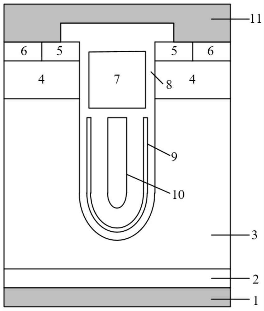
Figure 1 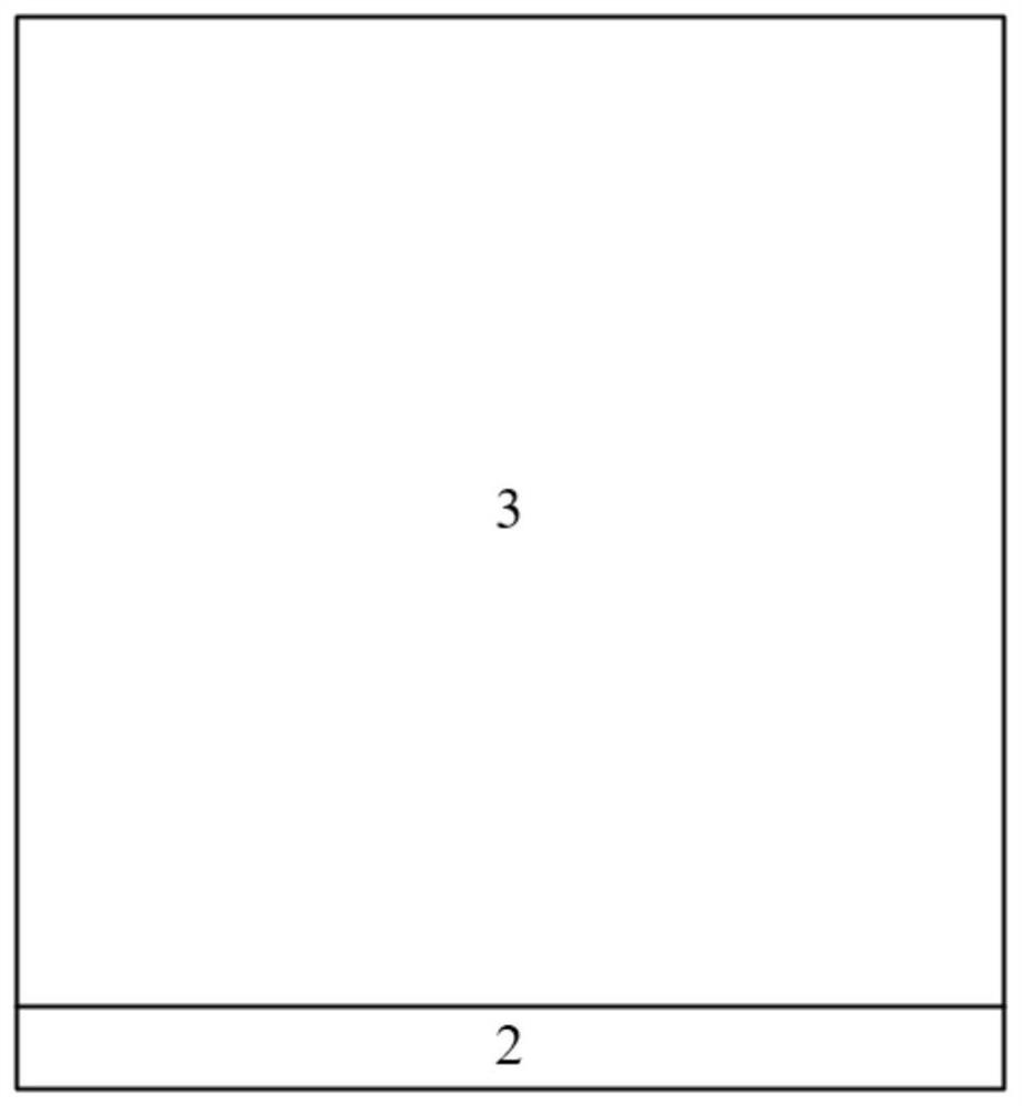
Figure 2 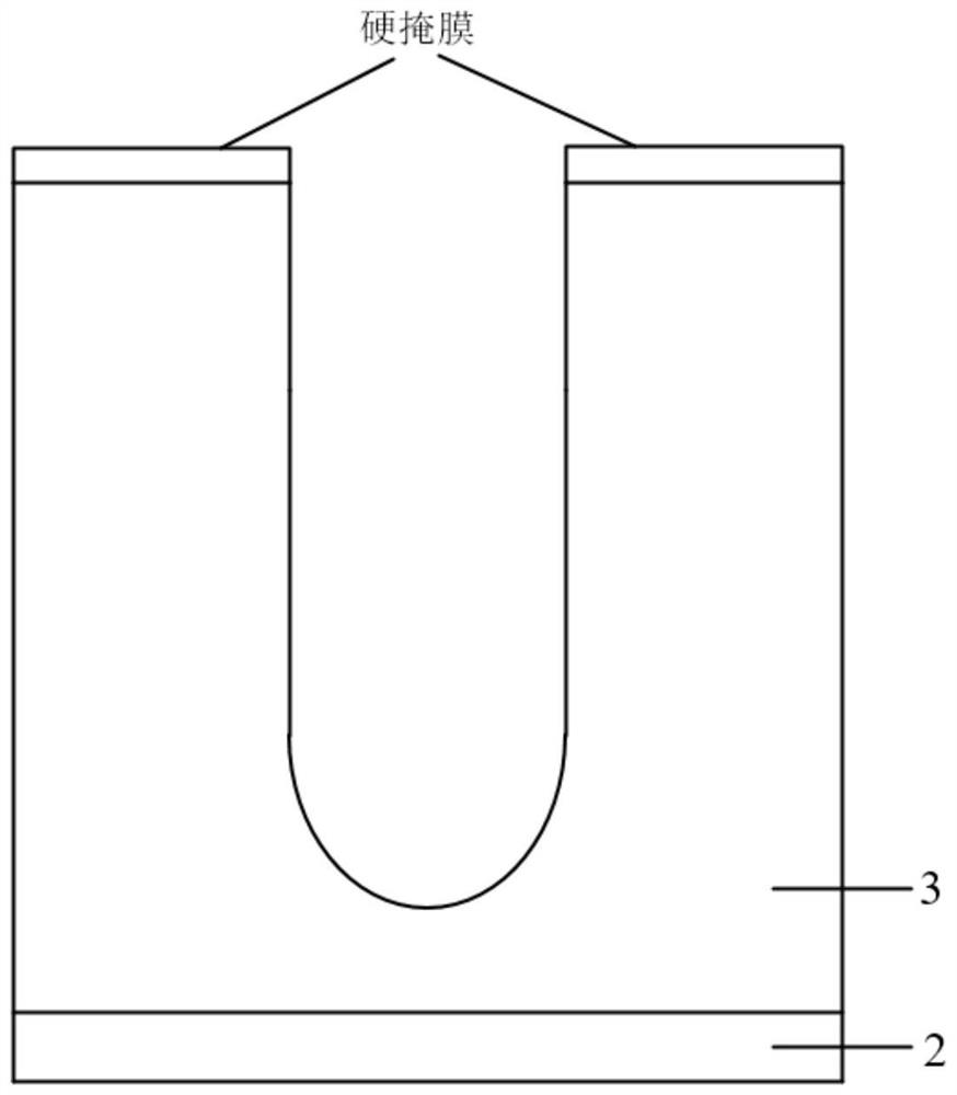
Figure 3
Abstract
Description
technical field
[0001] The invention belongs to the technical field of power semiconductors, and in particular relates to an SGT device with a silicon nitride barrier layer and a preparation method thereof. Background technique
[0002] Since Dr. Zeng Jun of Fairchild Semiconductor proposed Shield-gate VDMOS in 2003, this device with low specific on-resistance and low gate charge has attracted widespread attention. The device introduces a new electrode in the conventional groove gate VDMOS groove, which can be used as a field plate-assisted depletion device in the drift region of the carrier to reduce the specific on-resistance of the device, and can also act as a shield to reduce the interaction between the gate electrode and the drain electrode. The stack area reduces the Miller capacitance of the device and reduces the gate charge. Compared with traditional VDMOS devices, shielded gate VDMOS devices have the advantages of low power loss, small parasitic capacitance, fast...
Examples
Embodiment
[0040] A SGT device with a silicon nitride barrier layer, characterized in that it includes a metallized drain 1, an N+ substrate 2, an N-drift region 3, and a metallized source 11 stacked sequentially from bottom to top;
[0041] The N-drift region 3 has a trench gate structure, a P-type doped region 4, a P+ heavily doped region 6 and an N+ heavily doped region 5;
[0042] The trench gate structure includes an oxide layer 8, a control gate electrode 7 located inside the oxide layer 8, a silicon nitride barrier layer 9 and a shielded gate electrode 10, and the silicon nitride barrier layer 9 and the shielded gate electrode 10 are located on the control gate electrode 7 Below, the control gate electrode 7 and the shielding gate electrode 10 are not in contact, the silicon nitride barrier layer 9 is U-shaped, and the silicon nitride barrier layer 9 is located in the oxide layer 8 on the left and right sides and the bottom of the shielding gate electrode 10;
[0043] The P-type d...