
A planar metal oxide semiconductor diode with adjustable turn-on voltage
A technology of oxide semiconductor and turn-on voltage, which is applied in the direction of semiconductor devices, circuits, electrical components, etc., can solve problems such as limiting the application of devices, and achieve small conduction voltage drop, small reverse leakage current, and adjustable turn-on voltage Effect
Patent Information
- Authority / Receiving Office
- CN · China
- Patent Type
- Patents(China)
- Current Assignee / Owner
- Publication Date
- 2019-03-29
- Estimated Expiration
- Not applicable · inactive patent
Smart Images
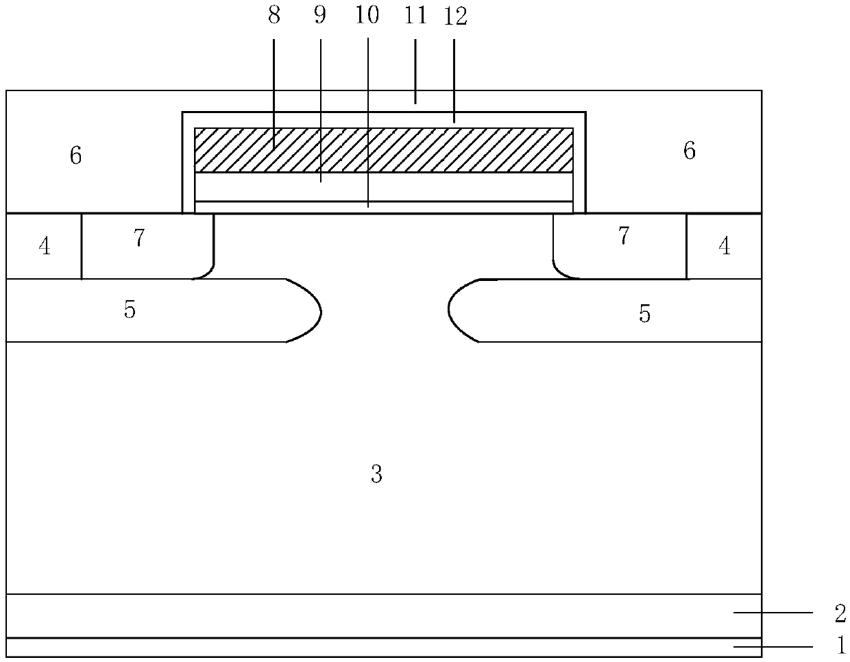
Figure 1 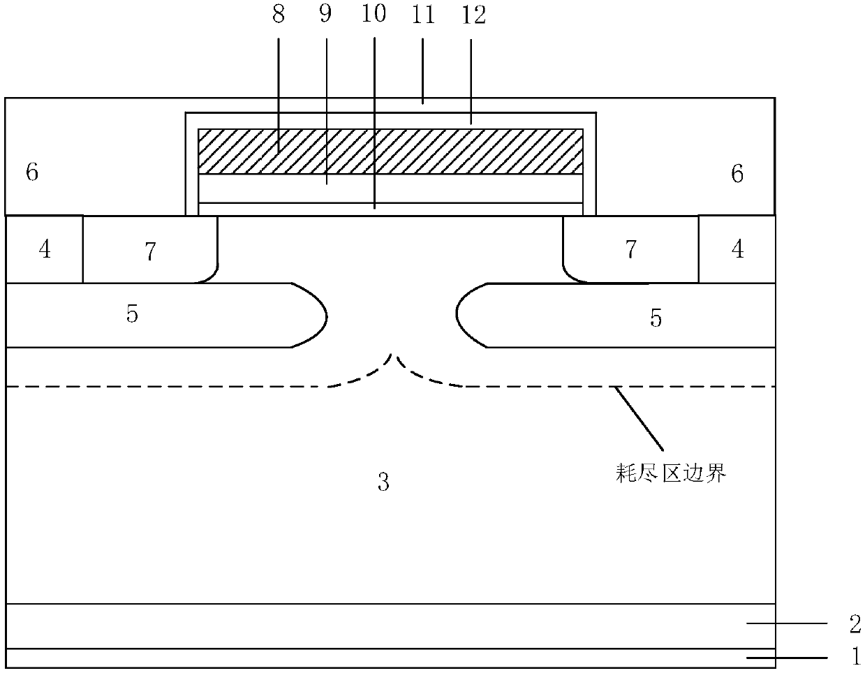
Figure 2 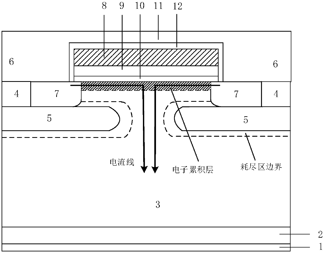
Figure 3
Abstract
Description
technical field
[0001] The invention relates to semiconductor technology, in particular to a planar metal oxide semiconductor diode with adjustable turn-on voltage. Background technique
[0002] Diodes are one of the most commonly used electronic components. Traditional rectifier diodes are mainly Schottky rectifiers and PN junction rectifiers. Among them, the PN junction diode can withstand a high reverse blocking voltage and has good stability, but its forward conduction voltage drop is relatively large, and its reverse recovery time is relatively long. Schottky diodes are manufactured using the principle of metal-semiconductor junctions formed by metal-semiconductor contacts, and the on-state voltage drop is low. Due to the conduction of unipolar carriers, Schottky diodes have no excess minority carrier accumulation during forward conduction, and the reverse recovery is relatively fast. However, the reverse breakdown voltage of the Schottky diode is low, the reverse lea...
Examples
Embodiment Construction
[0013] The present invention is described in detail below in conjunction with accompanying drawing
[0014] Such as figure 1 As shown, a planar metal oxide semiconductor diode with adjustable turn-on voltage of the present invention includes an N-type heavily doped single crystal silicon substrate 2, an N - the epitaxial layer 3 and the cathode electrode 1 located on the lower surface of the N-type heavily doped single crystal silicon substrate 2; the N-type epitaxial layer 3 has N-type heavily doped regions 7 on both sides of the upper layer, and the N-type heavily doped The lower surface of the region 7 is connected with a P-type buried layer 5; the side of the N-type heavily doped region 7 is a P-type heavily doped region 4; the middle part of the upper surface of the N- epitaxial layer 3 has a planar gate structure, and the planar The gate structure includes a silicon dioxide gate oxide layer 10, a nitride dielectric layer 9 and a polysilicon gate electrode 8; both sides ...