
Diode structure
a diode and structure technology, applied in the direction of basic electric elements, electrical equipment, semiconductor devices, etc., can solve the negative influence of the efficiency of the charge pump, and achieve the effect of reducing leakage current, improving performance, and increasing forward curren
Patent Information
- Authority / Receiving Office
- US · United States
- Patent Type
- Patents(United States)
- Current Assignee / Owner
- Publication Date
- 2018-06-12
Smart Images
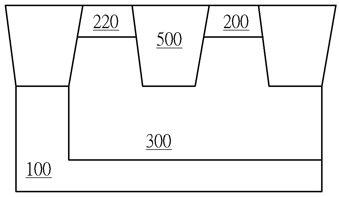
Figure 1 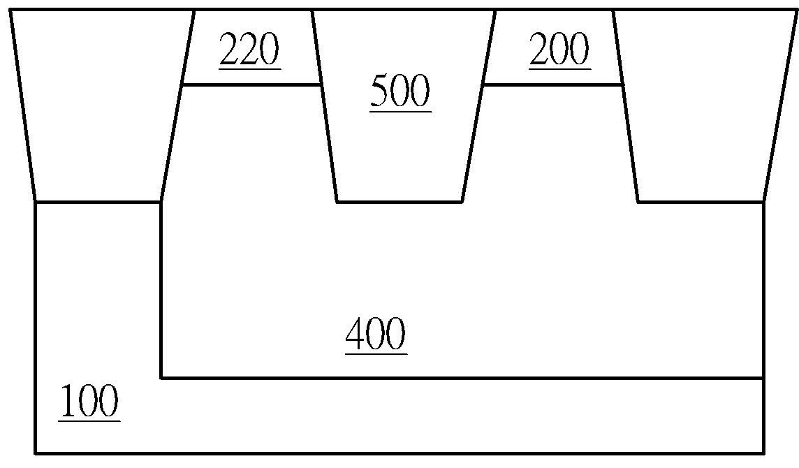
Figure 2 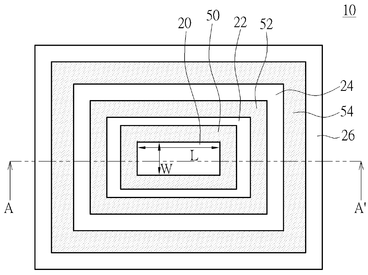
Figure 3
Abstract
Description
BACKGROUND OF THE INVENTION
[0001] 1. Field of the Invention
[0002] The present invention generally relates to a diode structure. More particularly, the present invention relates to a diode with multiple-concentric-rectangular-ring structure.
[0003] 2. Description of the Prior Art
[0004] A charge pump is a kind of circuit design which is very common in a circuit system. The charge pump is able to generate an output voltage greater in magnitude than the input voltage. The charge pump is applied widely in different kind of chips. For example, a charge pump is usually integrated in an electrical erasable programmable read only memory (EEPROM), which usually needs a voltage for the programming and erasing operations higher than the voltage available from the peripheral circuit. The integrated charge pump may multiply the voltage from the circuit, to provide an appropriate voltage for the programming and erasing operations of the memory.
[0005] With the integration of the semiconductor manufacturi...
Examples
Embodiment Construction
[0026]The present invention will now be described with reference to the attached drawings to provide a thorough understanding. Furthermore, some system configurations and process steps are not disclosed in detail, as these should be well-known to those skilled in the art. Other embodiments maybe utilized, and structural, logical, and electrical changes may be made without departing from the scope of the present invention.
[0027]FIG. 1 and FIG. 2 are the schematic cross-sectional diagrams of two types of conventional diodes of the prior art.
[0028]Please refer to FIG. 1, which is the cross-sectional diagram of an N+ / PW diode. The heavily doped N+ doping region 200 and the P+ doping region 220 are disposed in the P well 300, and are separated by the isolation structure 500. When the diode is forward-biased, that is, when the electrical potential of the P+ doping region 220 is relatively positive with respect to the electrical potential of the N+ doping region 200, the potential barrier ...