
Semiconductor device and production method thereof
A semiconductor and device technology, applied in the field of semiconductor devices and their production, can solve the problems of inability to realize high-voltage resistant semiconductor devices, degradation of gate or anode performance, and increase of reverse leakage, so as to improve withstand voltage characteristics and reduce potential barriers The effect of height and reverse bias voltage reduction
Patent Information
- Authority / Receiving Office
- CN · China
- Patent Type
- Applications(China)
- Current Assignee / Owner
- Publication Date
- 2019-05-21
Smart Images
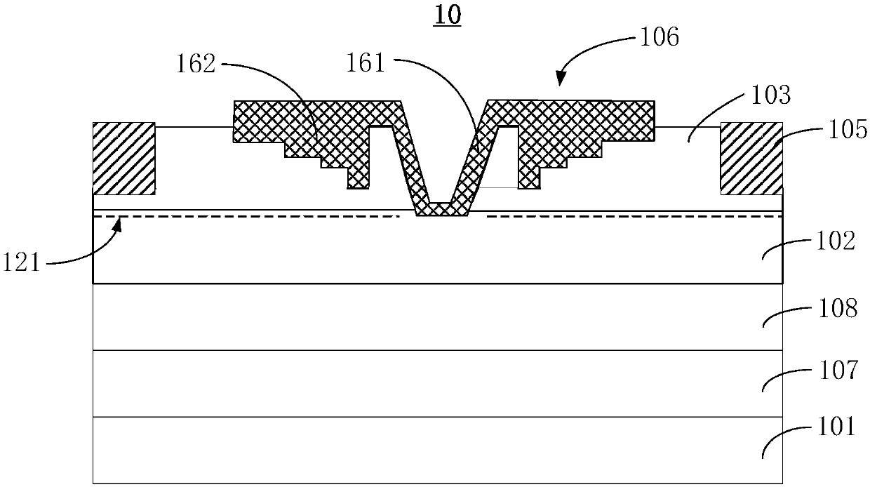
Figure 1 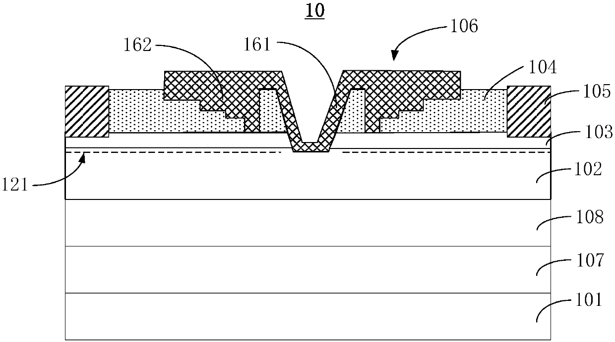
Figure 2 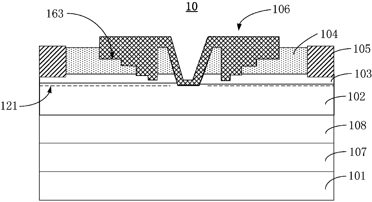
Figure 3
Abstract
Description
technical field
[0001] The present invention relates to the technical field of semiconductors, in particular to a semiconductor device and a manufacturing method thereof. Background technique
[0002] In the application field of high-voltage switches, it is hoped that semiconductor devices have the characteristics of small reverse leakage and large reverse withstand voltage. Semiconductor devices based on wide bandgap semiconductor materials, such as gallium nitride, silicon carbide, and diamond, have gradually become research hotspots.
[0003] For example, gallium nitride materials are mainly obtained by epitaxial growth on heterogeneous materials, based on the two-dimensional electron gas channel with high electron mobility in the horizontal direction formed by the AlGaN / GaN heterostructure. Mobility devices (HEMTs) have been widely used in radio frequency and power electronics. On the one hand, gallium nitride is a wide bandgap semiconductor material with a critical br...
Examples
Embodiment Construction
[0048] The following will clearly and completely describe the technical solutions in the embodiments of the present invention with reference to the accompanying drawings in the embodiments of the present invention. Obviously, the described embodiments are only some, not all, embodiments of the present invention. The components of the embodiments of the invention generally described and illustrated in the figures herein may be arranged and designed in a variety of different configurations. Accordingly, the following detailed description of the embodiments of the invention provided in the accompanying drawings is not intended to limit the scope of the claimed invention, but merely represents selected embodiments of the invention. Based on the embodiments of the present invention, all other embodiments obtained by those skilled in the art without making creative efforts belong to the protection scope of the present invention.
[0049] It should be noted that like numerals and let...