
Epitaxial structure and low on-voltage transistor
An epitaxial structure and transistor technology, which is applied in the direction of semiconductor devices, circuits, electrical components, etc., can solve the problems of large turn-on voltage of transistors, difficulty in reducing, and high power consumption of devices, and achieve reduced turn-on voltage, reduced peak effect, and reduced The effect of power consumption
Patent Information
- Authority / Receiving Office
- CN · China
- Current Assignee / Owner
- Publication Date
- 2019-12-24
Smart Images
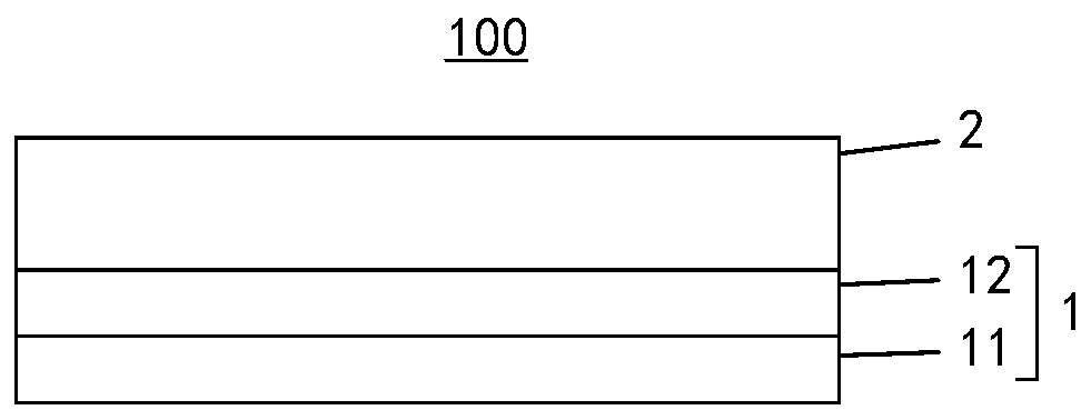
Figure 1 
Figure 2 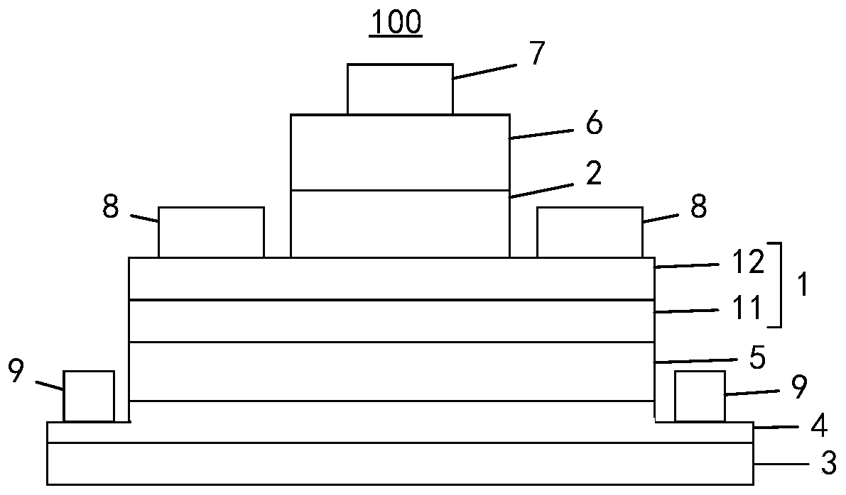
Figure 3
Abstract
Description
technical field
[0001] The present application relates to the field of semiconductor and communication technologies, and in particular, relates to an epitaxial structure and a low turn-on voltage transistor. Background technique
[0002] In power amplifiers currently used in 3G or 4G, power added efficiency (referred to as "PAE") is a very important parameter. PAE is defined as the ratio of the difference between the output power Pout and the input power Pin to the DC input power Pdc, namely: (Pout-Pin) / Pdc. PAE is a pointer indicating the quality of PA efficiency, and the larger the value, the more power loss of the power amplifier can be suppressed. To improve the DC power consumption, the first step is to reduce the conduction voltage (Von), the knee voltage ("Vk" for short) and the offset voltage ("Voff" for short). However, the turn-on voltage of the transistor used in the existing power amplifier is too large, and it is difficult to reduce, resulting in high power co...
Examples
no. 1 example
[0033] see figure 1 , this embodiment provides an epitaxial structure 100 , including a composite base electrode layer 1 and an emitter layer 2 fabricated based on the composite base electrode layer 1 .
[0034] Wherein, the composite base electrode layer 1 is a double-layer material structure, including a first base electrode layer 11 and a second base electrode layer 12 made on the basis of the first base electrode layer 11 . The material of the first base electrode layer 11 includes GaAs, and the material of the second base electrode layer 12 includes In x Ga 1-x As. In x Ga 1-x Compared with GaAs, As is a material with a lower energy gap. When used in transistors, it can improve the effect of conduction band spiking, reduce the turn-on voltage of transistors, and reduce power consumption.
[0035] In the second base electrode layer 12, in the direction close to the emitter layer 2, the In content is equal, that is, figure 1 The In content of the second base electrode...
no. 2 example
[0051] This embodiment provides an epitaxial structure 100 , which differs from the epitaxial structure 100 provided in the first embodiment in that the composition of In in the second base electrode layer 12 is different.
[0052] The epitaxial structure 100 includes a composite base electrode layer 1 and an emitter layer 2 . The composite base electrode layer 1 is a double-layer material structure, including a first base electrode layer 11 and a second base electrode layer 12 made on the basis of the first base electrode layer 11 . Wherein, the first base electrode layer 11 and the emitter layer 2 are the same as those in the first embodiment, and will not be repeated here.
[0053] In in the second base electrode layer 12 x Ga 1-x As, in the direction close to the emitter layer 2, the value of x gradually increases. That is to say, figure 1 In the second base electrode layer 12, the In content gradually increases as the thickness increases, and the increasing speed can ...
no. 3 example
[0059] This embodiment provides an epitaxial structure 100 , which is further designed as an epitaxial structure 100 suitable for HBT (Heterojunction Bipolar Transistor) on the basis of the epitaxial structure 100 provided in the first embodiment or the second embodiment.
[0060] see image 3 , the epitaxial structure 100 includes a substrate 3 , a sub-collector layer 4 , a collector layer 5 , a composite base electrode layer 1 , an emitter layer 2 and a cap layer 6 grown sequentially from bottom to top. Wherein, the composite base electrode layer 1 and the emitter layer 2 adopt the structure in the first embodiment or the second embodiment.
[0061] In addition, an emitter metal contact layer 7 is disposed above the emitter layer 2, and the emitter metal contact layer 7 covers the cap layer 6 and is in ohmic contact with the emitter layer 2, wherein the cap layer 6 is etched with a A via through which the emitter metal contact layer 7 passes. A base electrode metal contact...