
Field effect transistor, marginal structure and relative manufacture method
A technology of field effect transistors and transistor units, applied in semiconductor/solid-state device manufacturing, semiconductor devices, electrical components, etc., capable of solving reliability and durability reduction, field effect transistor 10 reverse breakdown voltage drift, and affecting field effects Problems such as the service life of the transistor 10 are achieved to improve the service life and solve the effect of easy breakdown
Patent Information
- Authority / Receiving Office
- CN · China
- Patent Type
- Applications(China)
- Current Assignee / Owner
- Publication Date
- 2013-08-28
Smart Images
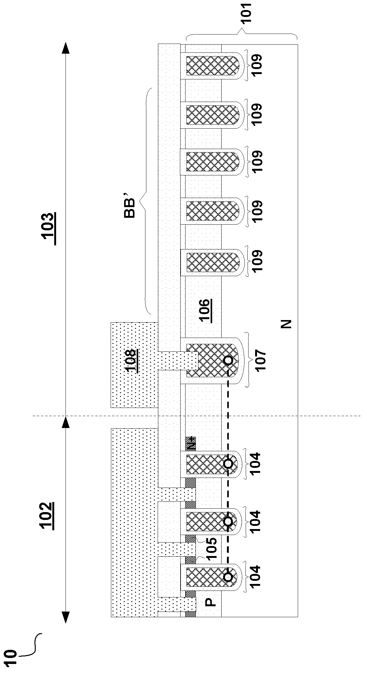
Figure 1 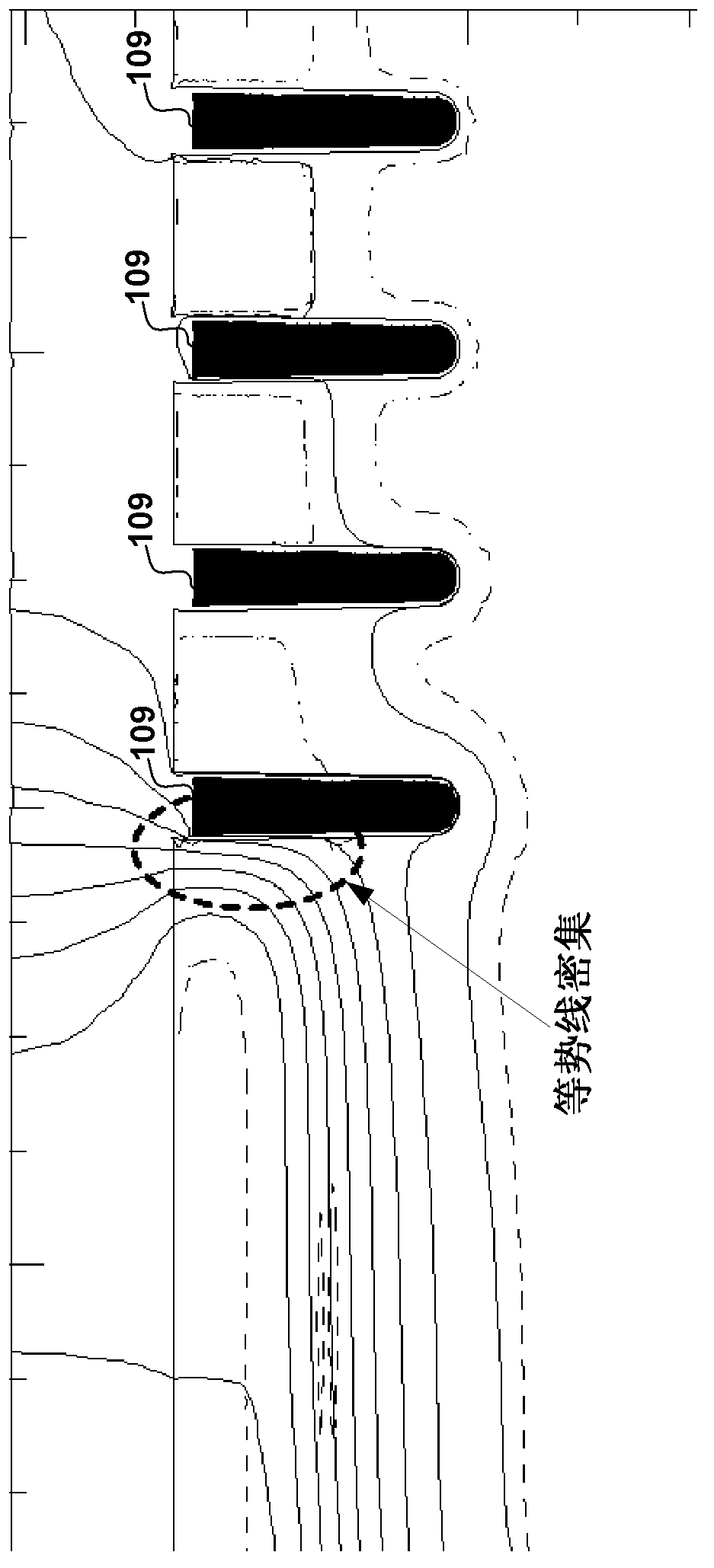
Figure 2 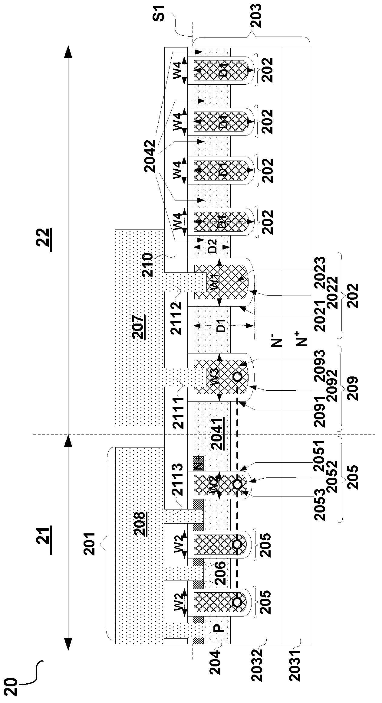
Figure 3
Abstract
Description
technical field
[0001] Embodiments of the present disclosure relate to semiconductor devices, particularly but not limited to field effect transistors and methods of manufacturing the same. Background technique
[0002] Semiconductor devices such as Metal Oxide Semiconductor Field Effect Transistor (MOSFET), Junction Field Effect Transistor (JFET) and Double Diffused Metal Oxide Semiconductor Field Effect Transistor (DMOS) have been widely used in the electronics industry. In some applications, such as power switches for switching voltage converters, field effect transistors should have good current handling capabilities, low on-resistance Rds ON , higher breakdown voltage BV and good safety and durability.
[0003] Field effect transistors such as MOSFETs, JFETs, DMOSs, etc. are usually fabricated on a semiconductor substrate and have an active cell area and an edge area. The effective cell area includes at least one field effect transistor unit, has a gate area, a source...
Examples
Embodiment Construction
[0026] Some embodiments of the present disclosure will be described in detail below with reference to the accompanying drawings. It should be understood, however, that these descriptions are exemplary only, and are not intended to limit the scope of the present disclosure. Also, descriptions of well-known structures and techniques are omitted in the following description to avoid unnecessarily obscuring the concepts of the present disclosure.
[0027] In the following description, some specific details, such as the specific circuit structure, device structure, process steps and specific parameters of these circuits, devices and processes in the embodiments, are used to provide a better understanding of the embodiments of the present disclosure . It will be understood by those skilled in the art that the embodiments of the present disclosure may be practiced even without some details or in combination with other methods, elements, materials, and the like.
[0028] In the desc...